Measurement Computing CIO-DAS16/M1 User Manual
Page 24
20
Pacer Clock Data & Control Registers
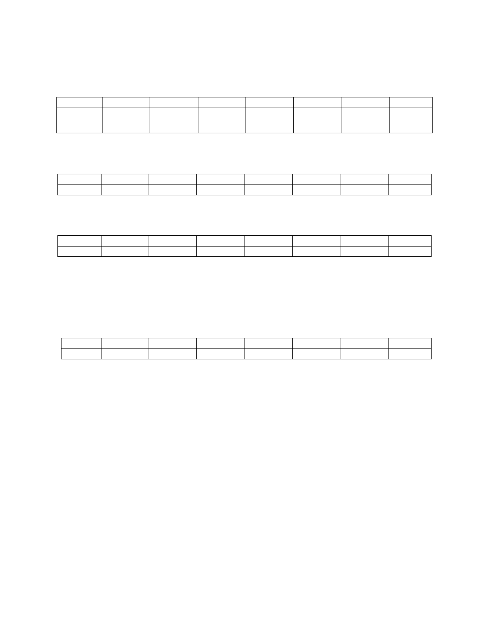
8254 COUNTER 0 DATA - User accessible counter.
BASE ADDRESS + C
7
6
5
4
3
2
1
0
D8
D7
D6
D5
D4
D3
D2
D1
8254 COUNTER 1 DATA - A/D pacer upper 1/2
BASE ADDRESS + D
7
6
5
4
3
2
1
0
D8
D7
D6
D5
D4
D3
D2
D1
8254 COUNTER 2 DATA - A/D pacer lower 1/2
BASE ADDRESS + E
7
6
5
4
3
2
1
0
D8
D7
D6
D5
D4
D3
D2
D1
The three 8254 counter/timer data registers can be written to and read from. Because each counter will
count as high as 65,536, it is clear that loading or reading the counter data must be a multi-step process.
The operation of the 8254 is explained in the section on the counter/time and the Intel 8254 data sheet.
8254 COUNTER CONTROL
BASE ADDRESS + F
7
6
5
4
3
2
1
0
D8
D7
D6
D5
D4
D3
D2
D1
This register controls operation and loading/reading of the counters. The configuration of the 8254 codes
which control the 8254 chip is explained in the section on the counter timer and the Intel 8254 data sheet.
4.6.9
Digital I/O and Counter Control & Data Registers
These registers control the 82C55 digital I/O chip and a 82C54 counter chip supplying user counters 0, 1
and 2. The three counter’s signals are available on the 40-pin digital connector.
The 82C55 requires three data and one control register occupying four consecutive I/O locations.
The 82C54 requires three data and one control register occupying four consecutive I/O locations.
The first address of the 82C55 is fixed at Base + 400h (Table 4-4). The base address is determined by
setting a bank of switches on the board.