4 functional description, 1 block diagram, 2 module description – Sundance SMT329 User Manual
Page 10: Functional description, Block diagram, Module description, Figure 1: smt329 architecture
Advertising
4 Functional Description
4.1 Block Diagram
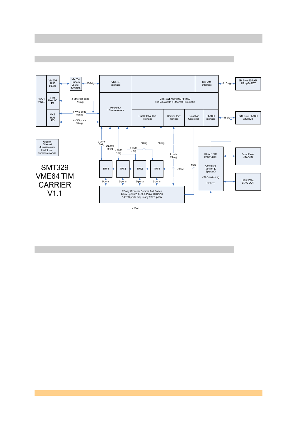
Figure 1: SMT329 Architecture
4.2 Module Description
Figure 1 shows the SMT329 block diagram. There are 4 single width or 2 double width TIM
sites. All communications apart from the comms port switching are routed through the Xilinx
Virtex4 fpga, including all VME and SRAM i/o. Comms port cross bar switching is
performed by a Xilinx Spartan3. Loading the configuration data into the 2 fpgas and
managing the JTAG interface are performed by a Xilinx CPLD.
User Manual SMT329
Last Edited: 09/02/2007 10:58:00
Advertising