4 vme interface, Vme interface – Sundance SMT329 User Manual
Page 22
4.4 VME Interface
The VME interface uses the P1 connector and the center row (B) of the P2 connector for
additional data and address lines. The interface forms a complete D8/16/32/64 master/slave.
The SMT329 does not support slot 0 operation or unaligned transfers.
Rows A and C of the P2 connector are connected to 4 of the Virtex4 RSL transmit receive
pairs. This allows the fitting of a rear transition PCB to support external high speed serial
interfaces such as 1M bit Ethernet, on both VME64 and legacy VME systems.
A central P0 connector is a factory fitted option which allows connection to a back plane
which supports the VXS standard. The P0 connector has 4 fixed RSL transmit receive pairs.
The VME64 bus is buffered with SN74VMEH22501A transceivers from TI which are specially
designed to be compliant with VME64,
2eVME protocols in VME64x (ANSI/VITA 1.1) and
2eSST protocols in VITA 1.5. With proper design of a 21-slot VME64 system, a designer can
achieve 320-Mbyte transfer rates on linear backplanes and, possibly up to 1-Gbyte/sec
transfer rates on the VME320 backplane.
For legacy VME systems without a 3.3 Volt supply,
SMT329 can be assembled with an on
board 3.3V PSU. In a legacy VME system the SMT329 does not guarantee to support 2eVME
or 2eSST and does not support VXS, but it does retain the four Gigabit Ethernet ports on the
P2 connector.
The use of high speed transfer modes (2eVME and 2eSST) on legacy backplanes VME is not
supported, and may or may not function reliably.
The VME master interface can be used by either TIM1 or TIM4 global bus, and by DMAA and
DMAB.
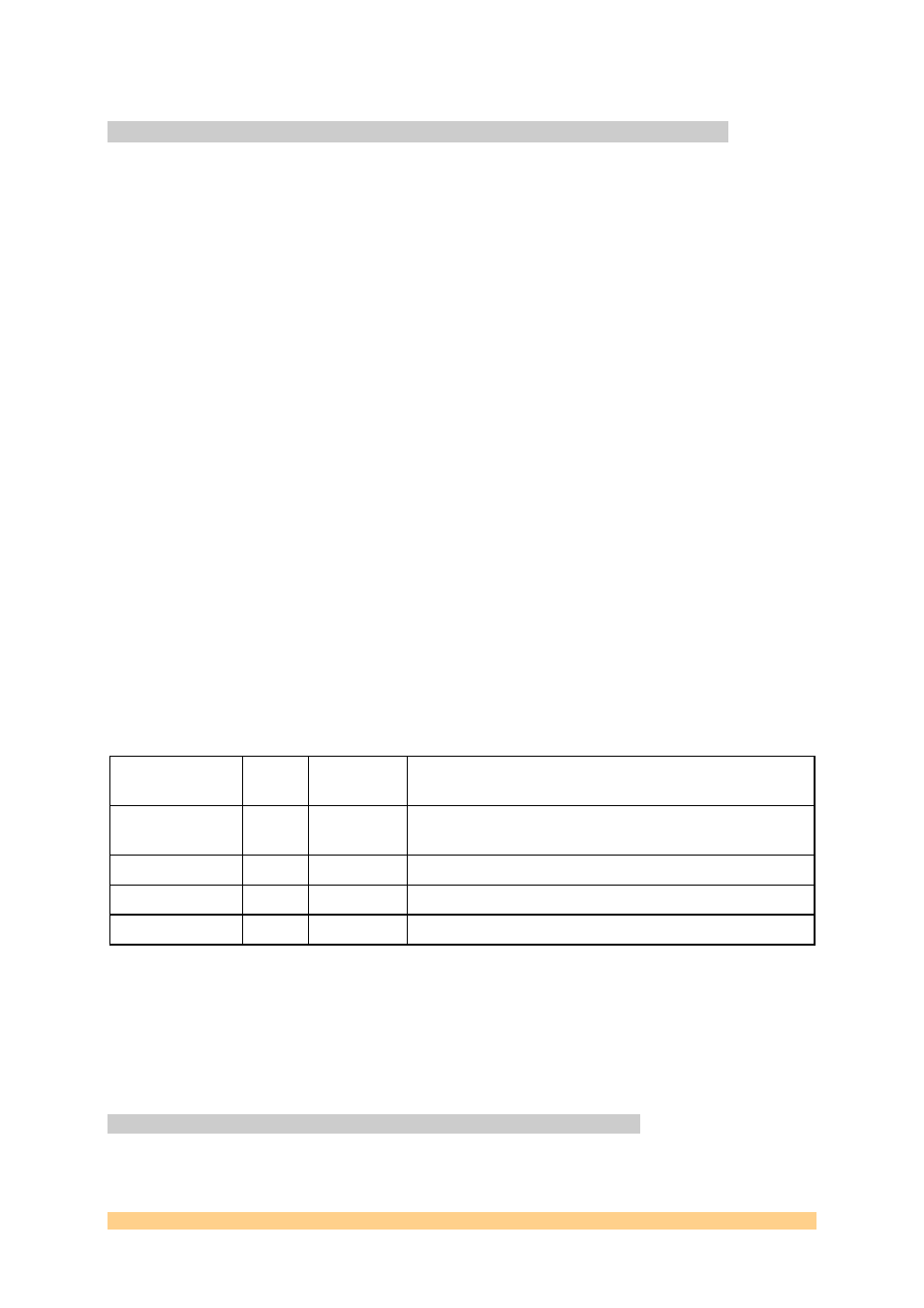
The SMT329 VME slave interface allows direct access by the current VME bus master to 7 out
of the 8 available SMT329 slaves, as shown in table 1 above. It has 3 separately decoded VME
bus address spaces, divided as follows:
Name VME
space
Size in
Bytes
Description
VME
configuration
A16
64
Identification and programmable base addresses
for I/O and SRAM. Board Reset.
I/O
A32
256
Comm-port, Board Reset, Control, Flash
I/O2 A32
768
DMA,
RSL
SRAM A32
8M
Static
Ram
The A16 VME configuration base address is set with an 8 way DIP switch labelled SW1. This
sets the value to compare to VME A6-A13, with VME A14-A15 always compared to 1 in order
to generate a board decode. This A16 address space contains board identification registers
and a pair of 16 bit registers which must be loaded with the base address of the I/O and
SRAM spaces.
4.4.1 VME slave interface to VME config and reset registers
User Manual SMT329
Page 22 of 52 Last
Edited:
09/02/2007
10:58:00