Using the rssi pin, The data output – Linx Technologies RXM-xxx-LR User Manual
Page 8
– –
– –
10
11
Using the RSSI Pin
The receiver’s Received Signal Strength Indicator (RSSI) line outputs a
voltage that is proportional to the incoming signal strength. This line has
a dynamic range of 80dB (typical) and can serve a variety of functions. It
should be noted that the RSSI levels and dynamic range will vary slightly
from part to part. It is also important to remember that RSSI output
indicates the strength of any in-band RF energy and not necessarily just
that from the intended transmitter; therefore, it should be used only to
qualify the level and presence of a signal.
The RSSI output can be utilized during testing or even as a product feature
to assess interference and channel quality by looking at the RSSI level
with all intended transmitters shut off. The RSSI output can also be used
in direction-finding applications, although there are many potential perils to
consider in such systems. Finally, it can be used to save system power by
“waking up” external circuitry when a transmission is received or crosses a
certain threshold. The RSSI output feature adds tremendous versatility for
the creative designer.
The Data Output
The CMOS-compatible data output is normally used to drive a digital
decoder IC or a microprocessor that is performing the data decoding. It
does not have a large current drive capability so is intended to drive high
impedance loads, such as microprocessor inputs or digital logic gates.
The receiver’s output may appear to switch randomly in the absence of a
transmitter. This is a result of random noise in the environment. This noise
can be handled in software by implementing a noise-tolerant protocol
as described in Application Note AN-00160. If a software solution is not
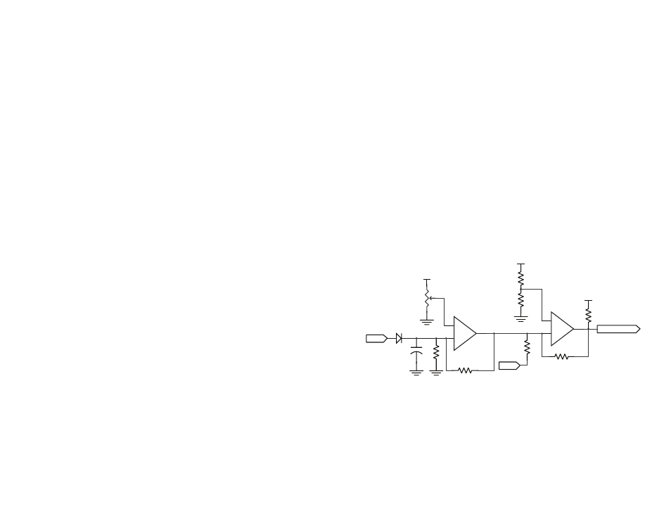
appropriate, the squelch circuit in Figure 13 can be used. This circuit uses
a potentiometer to set a voltage reference. If the RSSI level falls below this
reference then a comparator turns off the DATA line and stops the random
switching.
This circuit is good for reducing the amount of random noise that the
microcontroller must deal with, but it also reduces the sensitivity of the
receiver since the received signal level must now be higher. This reduction
in sensitivity also reduces the system range. By using a potentiometer the
designer can make a compromise between noise level and range.
+
-
+
U1
LMV393
R4
100k
R1
2M
R2
500k
C1
0.1
µ
D1
RSSI
DATA
Squelched Data
VCC
R3
5M
VCC
+
-
U1
LMV393
VCC
R5
1M
R6
1M
R7
2M
R8
10k
1
2
3
5
6
7
Figure 13: LR Series Receiver Squelch Circuit