Esd concerns, Power supply requirements, Protocol guidelines – Linx Technologies TXM-xxx-ES User Manual
Page 9
– –
– –
12
13
Power Supply Requirements
The module does not have an internal voltage
regulator; therefore it requires a clean,
well-regulated power source. While it is
preferable to power the unit from a battery, it can
also be operated from a power supply as long
as noise is less than 20mV. Power supply noise
can affect the transmitter modulation; therefore,
providing a clean power supply for the module
should be a high priority during design.
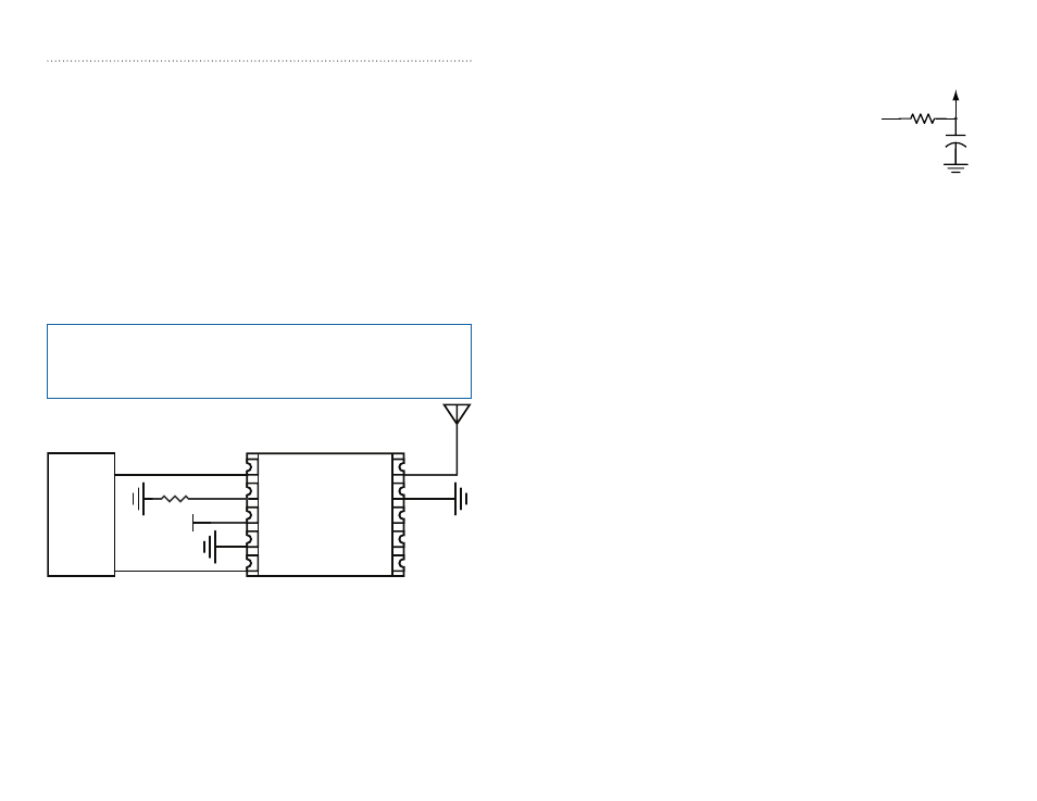
A 10
Ω
resistor in series with the supply followed by a 10µF tantalum
capacitor from VCC to ground will help in cases where the quality of supply
power is poor. Note that operation from 4.3 to 5.2 volts requires the use
of an external 270
Ω
resistor placed in series with the supply to prevent V
CC
from exceeding 4.0 volts, so the dropping resistor can take the place of
the 10
Ω
resistor in the supply filter. These values may need to be adjusted
depending on the noise present on the supply line.
Protocol Guidelines
While many RF solutions impose data formatting and balancing
requirements, Linx RF modules do not encode or packetize the signal
content in any manner. The received signal will be affected by such factors
as noise, edge jitter, and interference, but it is not purposefully manipulated
or altered by the modules. This gives the designer tremendous flexibility for
protocol design and interface.
Despite this transparency and ease of use, it must be recognized that there
are distinct differences between a wired and a wireless environment. Issues
such as interference and contention must be understood and allowed for
in the design process. To learn more about protocol considerations, we
suggest you read Linx Application Note AN-00160.
Errors from interference or changing signal conditions can cause corruption
of the data packet, so it is generally wise to structure the data being sent
into small packets. This allows errors to be managed without affecting large
amounts of data. A simple checksum or CRC could be used for basic error
detection. Once an error is detected, the protocol designer may wish to
simply discard the corrupt data or implement a more sophisticated scheme
to correct it.
+
10
Ω
10
µF
Vcc IN
Vcc TO
MODULE
Figure 14: Supply Filter
Using the ES Series Transmitter for Digital Applications
The ES Series transmitter is equally capable at accommodating digital data.
The transmitter’s input is high impedance (500k) and can be directly driven
by a wide variety of sources including microprocessors and encoder ICs.
When the transmitter will be used to transmit digital data, the DATA line is
best driven from a 3 to 5V source. The transmitter is designed to give an
average deviation of 115kHz with a 5V square wave input, and 75kHz with
3V square wave input. Either choice will achieve maximum performance.
Data adhering to different electrical level standards, such as RS-232,
will require buffering or conversion to logic level voltages. In the case of
RS-232, such buffering is easily handled with widely available ICs, such as
the MAX232, which is used on the ES Series Master Development System.
The Linx SDM-USB-QS can be used to convert between USB compliant
signals and logic level voltages.
ESD Concerns
The module has basic ESD protection built in, but in cases where the
antenna connection is exposed to the user it is a good idea to add
additional protection. A Transient Voltage Suppressor (TVS) diode, varistor
or similar component can be added to the antenna line. These should have
low capacitance and be designed for use on antennas. Protection on the
supply line is a good idea in designs that have a user-accessible power
port.
Note:
The RS-232 protocol is not a robust protocol for the noisy RF
environment. It can be used for very short range links, but is subject
to interference and does not contain any error detection or correction.
Please see the Protocol Guidelines section for more information.
µ
PDN
LADJ
VCC
LO_V_D
/CLK SEL
/CLK
GND
DATA
ANT
GND
1
2
3
4
5
6
7
8
9
10
GPIO
GPIO
VCC
Figure 13: ES Series Transmitter Typical Application Circuit