Ddio input register (full-rate or half-rate) – Altera GPIO User Manual
Page 18
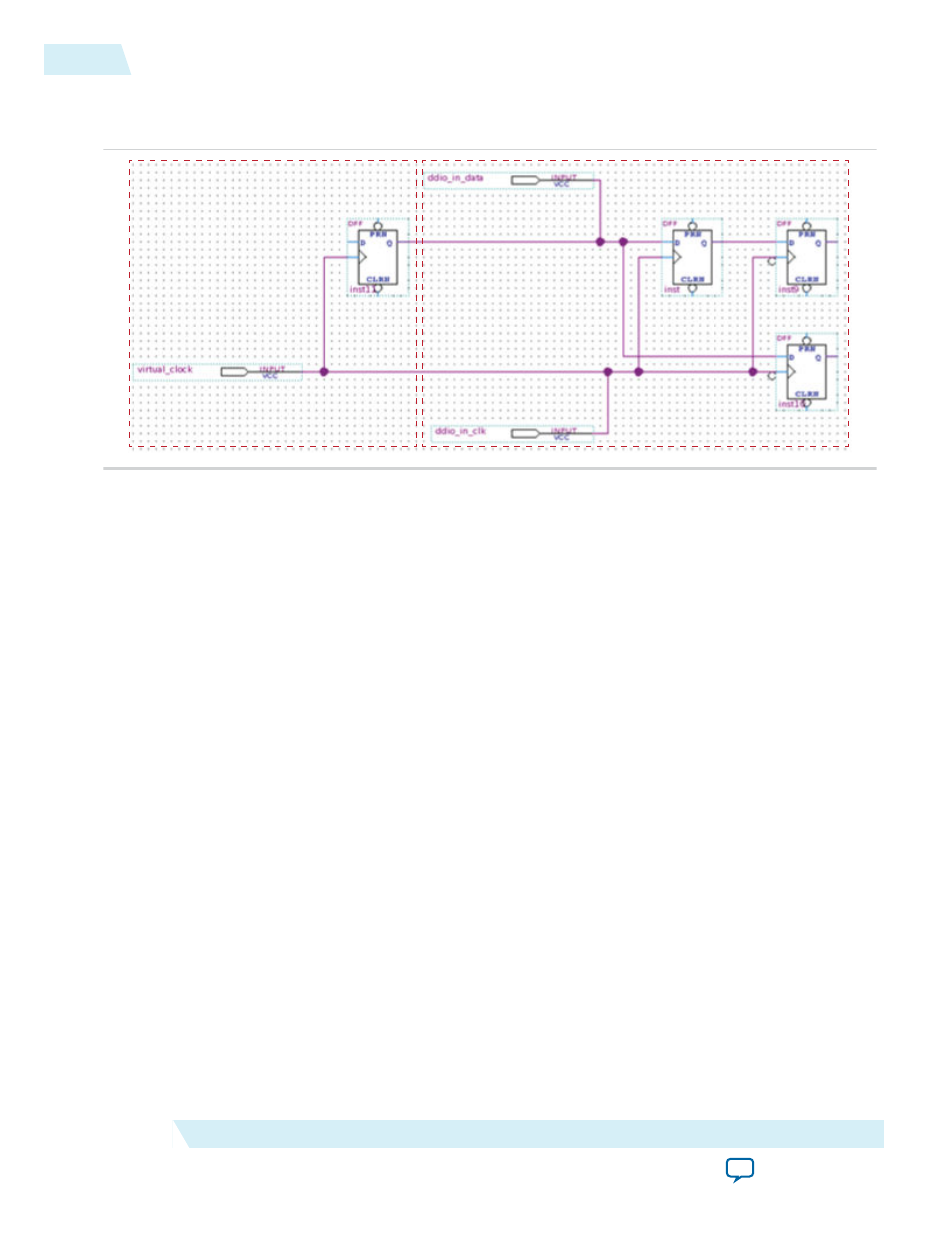
DDIO Input Register (Full-Rate or Half-Rate)
Figure 12: DDIO Input Register (Full-Rate or Half-Rate)
Outside FPGA
FPGA
The input side of full-rate and half-rate DDIO is the same. You can properly constrain the system by
using a virtual clock to model the off-chip transmitter to the FPGA.
create_clock
These SDC commands create the clock settings for the virtual and the DDIO clock.
create_clock -name virtual_clock -period "200 MHz"
create_clock -name ddio_in_clk -period "200 MHz" ddio_in_clk
set_input_delay
These
set_input_delay
commands instruct the TimeQuest timing analyzer to analyze the positive clock
edge and the negative clock edge of the transfer. Note the "-add_delay" in the second set_input_delay
command:
set_input_delay -clock virtual_clock 0.25 ddio_in_data
set_input_delay -add_delay -clock_fall -clock virtual_clock 0.25 ddio_in_data
set_false_path
These
set_false_path
commands instruct the TimeQuest timing analyzer to ignore the positive clock
edge to the negative edge triggered register and the negative clock edge to the positive edge triggered
register:
set_false_path -fall_from virtual_clock -rise_to ddio_in_clk
set_false_path -rise_from virtual_clock -fall_to ddio_in_clk
18
DDIO Input Register (Full-Rate or Half-Rate)
ug-altera_gpio
2014.08.18
Altera Corporation
Altera GPIO IP Core User Guide