Altera GPIO User Manual
Page 7
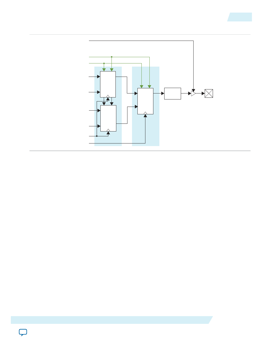
Figure 4: Output Path (Simplified View)
PAD
ACLR_N
APRE_N
DATAOUT[0]
DATAOUT[2]
DATAOUT[1]
DATAOUT[3]
CLK_HR
CLK_FR
DDIO
OUT
DDIO
OUT
DDIO
OUT
Delay
Element
HR
FR
OE
from Output
Enable Path
The simplified view of a GPIO output path is similar to the input path (refer to
). The output
delay element sends data to the pad through the output buffer.
Note: The Altera GPIO IP core does not support dynamic calibration of the input path. For applications
requiring dynamic calibration of the output path, refer to the
.
Note: When you set the Register mode option to Simple register, the full-rate DDIO works as a simple
register.
Note: When you set the Register Mode option to Simple register, the Fitter chooses whether to pack the
register in the I/O or implement the register in the core, depending on the area and timing trade-
offs.
You can select a combination of half-rate, full-rate DDIOs, and simple register using programmable
bypass multiplexers to implement the following four output modes:
• Bypass—data goes from the core straight to the delay element, bypassing all DDIOs.
• Packed Register—full-rate DDIO operates as a register, bypassing half-rate DDIOs.
• DDIO output mode, Full-Rate—full-rate DDIO operates as a regular DDIO, bypassing half-rate
DDIOs.
• DDIO output, Half-Rate—full-rate DDIO operates as a regular DDIO. Half-rate DDIOs convert data
from full-rate to half-rate.
All DDIOs share the same asynchronous clear and preset signals when used. Half-rate and full-rate
DDIOs connect to separate clocks. When you use half-rate and full-rate DDIOs, the full-rate clock must
run at twice the half-rate frequency. You can use different phase relationships to meet timing require‐
ments.
ug-altera_gpio
2014.08.18
Output Path
7
Altera GPIO IP Core User Guide
Altera Corporation