Overview, Input path – Altera GPIO User Manual
Page 4
Advertising
Name
Values
Description
Separate input/output Clocks
Turn on, Turn off
Allows the Altera GPIO to use separate clocks for
input and output data paths.
Overview
The following figure shows the high-level view of a single-ended GPIO.
Figure 1: Single-Ended GPIO
Buffer
OEIN[1:0]
DATAIN[3:0]
Output
Path
GPIO
OE
Path
Input
Path
DATAOUT[3:0]
Core
Input Path
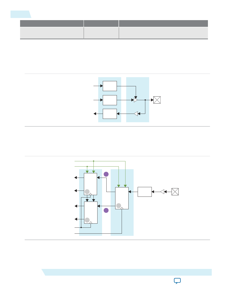
The following figure shows the simplified view of a single-ended GPIO input path.
Figure 2: Input Path (Simplified View)
PAD
ACLR_N
APRE_N
DATAOUT[0]
DATAOUT[2]
DATAOUT[1]
DATAOUT[3]
CLK_HR
CLK_FR
DDIO
IN
DDIO
IN
DDIO
IN
Delay
Element
HR
FR
B
A
1
3
2
The pad sends data to the input buffer, and the input buffer feeds the delay element.
4
Overview
ug-altera_gpio
2014.08.18
Altera Corporation
Altera GPIO IP Core User Guide
Advertising