Clock resource summary tab, Setting the receiver input clock parameters – Altera LVDS SERDES User Manual
Page 16
Description
Value
Parameter
Specifies the closest achievable
tx_outclock
phase
shift to the desired
tx_outclock
phase shift.
Legal values are
dependent on the
fclk and tx_
outclock
frequencies. Refer
to
Transmitter
Output Clock
Parameters
on
page 17.
Actual tx_outclock phase shift
(degrees)
Allows you to specify the ratio of the fast clock
frequency to the
outclock
frequency (for example,
the maximum number of serial transitions per
outclock cycle).
Legal values are
dependent on the
serialization
factor.
Tx_outclock division factor
Clock Resource Summary Tab
This tab in the parameter editor lists out all the required frequencies, phase shifts, and duty cycles of the
required clocks, including instructions on the required connections. This tab also shows how to configure
and connect an external PLL.
Setting the Receiver Input Clock Parameters
When using non-DPA mode, if you want the SERDES receiver to sample the source synchronous data, you
must specify the inclock relationship to the
rx_in
data. To do so, type a value in the Desired receiver inclock
phase shift (degrees) parameter. Legal values are evenly divisible by 45. If you enter an illegal value, the
actual phase shift will appear in Actual receiver inclock phase shift (degrees).
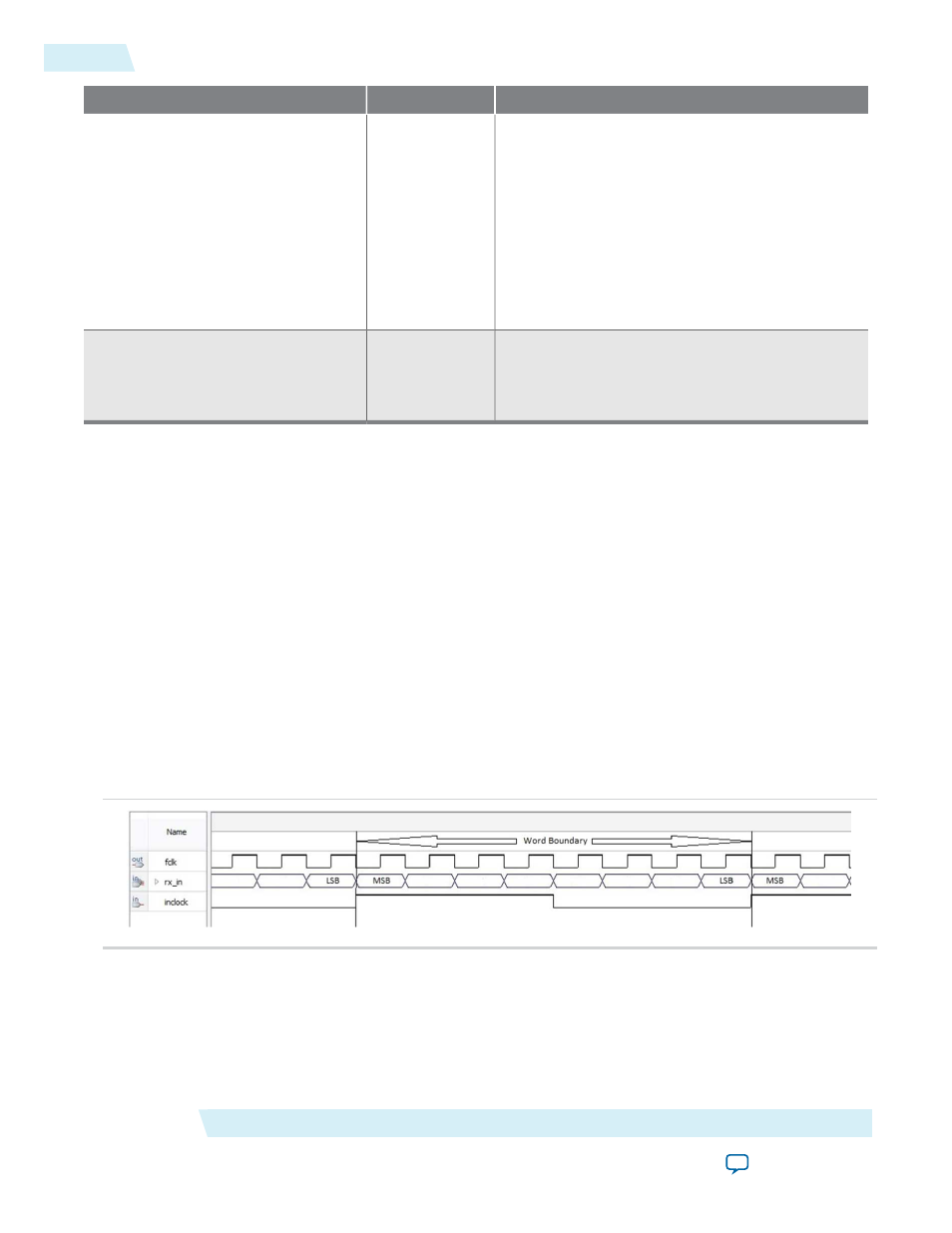
For rising inclock edge aligned interfaces to the
rx_in
data (
), select 0° as the desired receiver clock
phase shift. The PLL will be set with the required phase shift on
fclk
to center it at the SERDES receiver.
Figure 4: 0° Edge Aligned inclock x8 Deserializer Waveform With Single Rate Clock
The phase shift you specify will be relative to the
fclk
which operates at the serial data rate. Phase shift
values between 0° and 360° are used to specify the rising edge of the inclock within a single bit period. The
maximum phase shift value is determined by the following equation:
(Number of
fclk
periods per inclock period x 360) - 1
Altera LVDS SERDES IP Core User Guide
Altera Corporation
ug_altera_lvds
Clock Resource Summary Tab
16
2014.08.18