Altera LVDS SERDES User Manual
Page 9
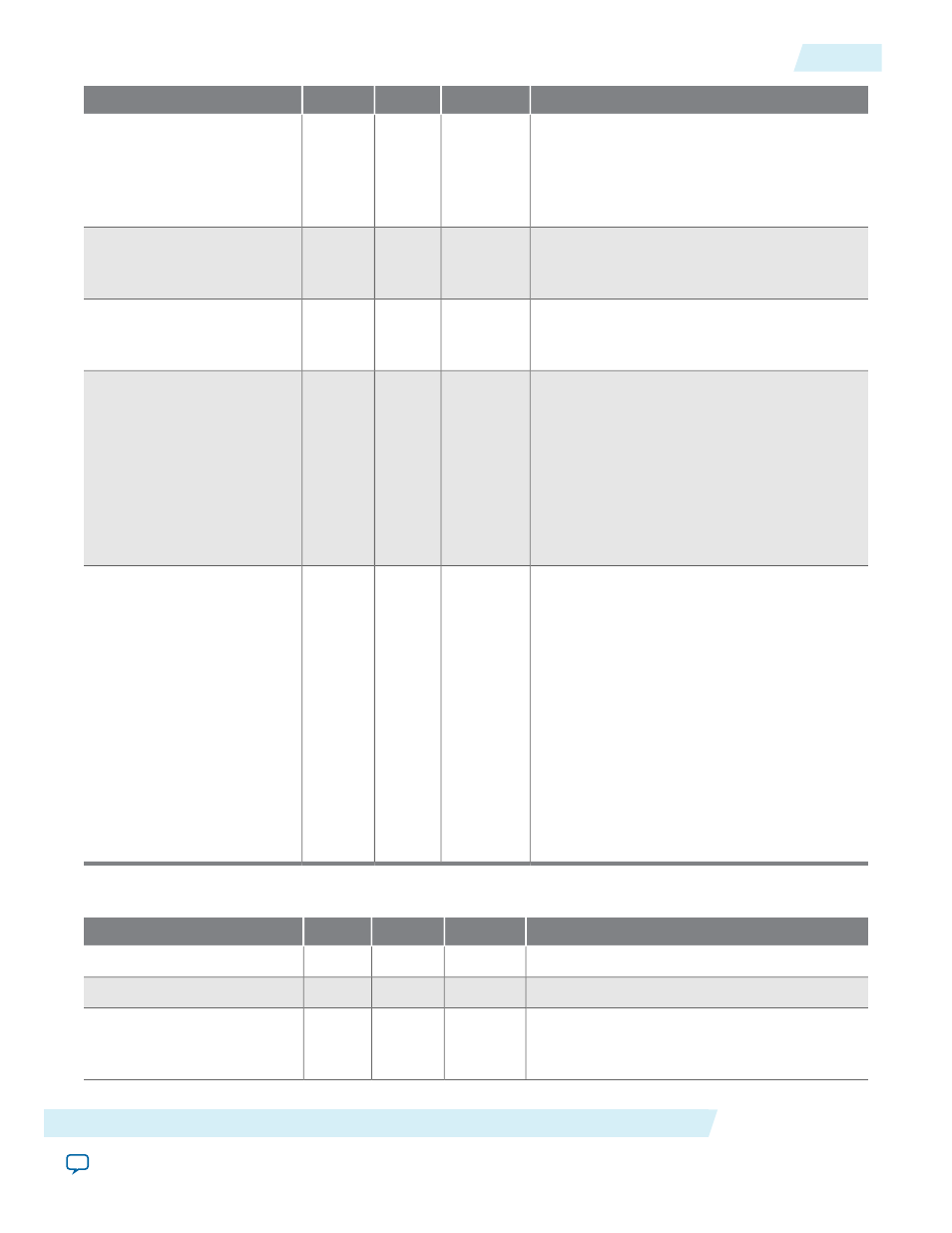
Description
Type
Direction
Width
Signal Name
Receiver parallel data output. Synchronous
to
rx_coreclock
in (DPA-FIFO and non-
DPA modes). In soft-CDR mode, each
channel has parallel data synchronous to its
rx_divfwdclk
.
Data
Output
N*J
rx_out
Bitslip rollover signal. High when the next
assertion of
rx_bitslip_ctrl
resets the serial
bit latency to
0
.
Control
Output
N
rx_bitslip_max
Core clock for RX interfaces provided by the
PLL. Not available when using an external
PLL.
Clock
Output
1
rx_coreclock
The per channel, divided clock with the ideal
DPA phase. The recovered slow clock for a
given channel. Applicable in soft-CDR mode
only. Because each channel may have a
different ideal sampling phase, the
rx_
divfwdclks
may not be edge-aligned with
each other. Each
rx_divfwdclk
must drive
the core logic with data from the same
channel.
Clock
Output
N
rx_divfwdclk
Asserted when the DPA block selects the ideal
phase. The Altera LVDS SERDES IP core
drives the
rx_dpa_locked
port. The DPA
logic asserts the
rx_dpa_locked
signal when
the signal settles on an ideal phase for that
given channel. The
rx_dpa_locked
port will
de-assert if the DPA moves two phases in the
same direction or if the DPA moves one
phase. The
rx_dpa_locked
signal will still
toggle when the
rx_dpa_hold
signal is
asserted, and should be ignored by user logic
when the
rx_dpa_hold
signal is asserted.
Applicable in DPA-FIFO and soft-CDR
modes only.
Control
Output
N
rx_dpa_locked
Table 4: TX Signals
Description
Type
Direction
Width
Signal Name
Parallel data from the core.
Data
Input
N*J
tx_in
LVDS serial output data.
Data
Output
N
tx_out
External reference clock (sent off chip via the
TX data path). Source-synchronous with
tx_
out
.
Clock
Output
1
tx_outclock
Altera Corporation
Altera LVDS SERDES IP Core User Guide
9
Signals
ug_altera_lvds
2014.08.18