Factory default switch settings, Factory default switch settings –2 – Altera Cyclone V E FPGA User Manual
Page 12
4–2
Chapter 4: Development Board Setup
Factory Default Switch Settings
Cyclone V E FPGA Development Kit
December 2014
Altera Corporation
User Guide
Factory Default Switch Settings
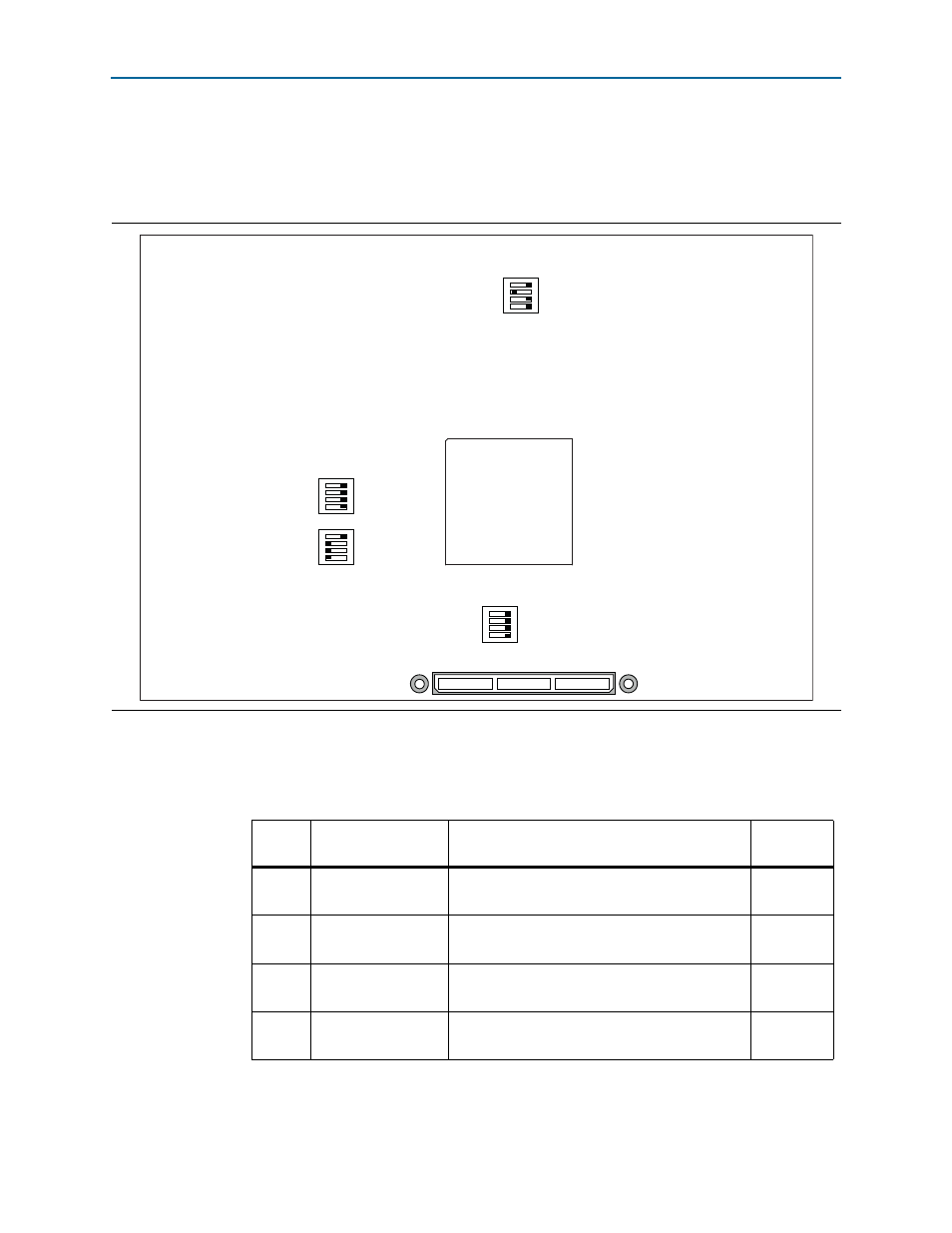
This section shows the factory switch settings (
) for the Cyclone V E FPGA
development board.
To restore the switches to their factory default settings, perform these steps:
1. Set the DIP switch bank (SW1) to match
and
.
Figure 4–1. Switch Locations and Default Settings
ON
SW1
ON
SW4
ON
SW3
ON
SW2
FPGA_MSEL0
FPGA_MSEL1
FPGA_MSEL2
FPGA_MSEL3
FAN_FORCE_ON
RESERVED
HSMC JTAG Enable
5M2210 JTAG Enable
CLK_SEL
CLK_EN
FACT_LOAD
SECURITY
Table 4–1. SW1 DIP Switch Settings
Switch
Board
Label
Function
Default
Position
1
FPGA_MSEL0
■
ON (0) = logic 0 is selected.
■
OFF (1) = logic 1 is selected.
ON
2
FPGA_MSEL1
■
ON (0) = logic 0 is selected.
■
OFF (1) = logic 1 is selected.
ON
3
FPGA_MSEL2
■
ON (0) = logic 0 is selected.
■
OFF (1) = logic 1 is selected.
ON
4
FPGA_MSEL3
■
ON (0) = logic 0 is selected.
■
OFF (1) = logic 1 is selected.
ON