Max v registers, Jtag chain, Max v registers –4 jtag chain –4 – Altera Cyclone V E FPGA User Manual
Page 20
6–4
Chapter 6: Board Test System
Using the Board Test System
Cyclone V E FPGA Development Kit
December 2014
Altera Corporation
User Guide
MAX V Registers
The MAX V registers control allows you to view and change the current MAX V
register values as described in
. Changes to the register values with the GUI
take effect immediately. For example, writing a 0 to SRST resets the board.
■
PSO
—Sets the MAX V PSO register. The following options are available:
■
Use PSR
—Allows the PSR to determine the page of flash memory to use for
FPGA reconfiguration.
■
Use PSS
—Allows the PSS to determine the page of flash memory to use for
FPGA reconfiguration.
■
PSR
—Sets the MAX V PSR register. The numerical values in the list corresponds
to the page of flash memory to load during FPGA reconfiguration. Refer to
for more information.
■
PSS
—Displays the MAX V PSS register value. Refer to
available options.
■
SRST
—Resets the system and reloads the FPGA with a design from flash memory
based on the other MAX V register values. Refer to
for more information.
1
Because the System Info tab requires that a specific design is running in the FPGA at
a specific clock speed, writing a 0 to SRST
or changing the PSO value can cause the
Board Test System to stop running.
JTAG Chain
The JTAG chain control shows all the devices currently in the JTAG chain. The
Cyclone V E device is always the first device in the chain. The JTAG chain is normally
mastered by the On-board USB-Blaster II.
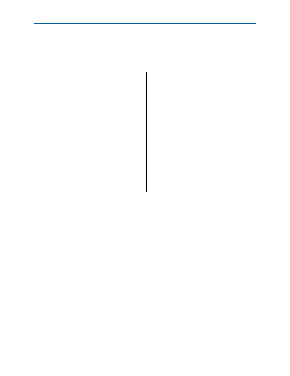
Table 6–1. MAX V Registers
Register Name
Read/Write
Capability
Description
System Reset
(SRST)
Write only
Set to 0 to initiate an FPGA reconfiguration.
Page Select Register
(PSR)
Read / Write
Determines which of the up to three (0-2) pages of flash
memory to use for FPGA reconfiguration. The flash memory
ships with pages 0 and 1 preconfigured.
Page Select Override
(PSO)
Read / Write
When set to 0, the value in PSR determines the page of
flash memory to use for FPGA reconfiguration. When set to
1, the value in PSS determines the page of flash memory to
use for FPGA reconfiguration.
Page Select Switch
(PSS)
Read only
Holds the current value of the illuminated PGM LED
(D25-D27) based on the following encoding:
■
0 = PGM LED (D25) and corresponds to the flash
memory page for the factory hardware design
■
1 = PGM LED (D26) and corresponds to the flash
memory page for the user hardware 1 design
■
2 = PGM LED (D27) and corresponds to the flash
memory page for the user hardware 2 design