Back to back read, 32-bit address and data – Avago Technologies LSI53C1000R User Manual
Page 311
Advertising
PCI and External Memory Interface Timing Diagrams
6-29
Version 2.2
Copyright © 2000–2003 by LSI Logic Corporation. All rights reserved.
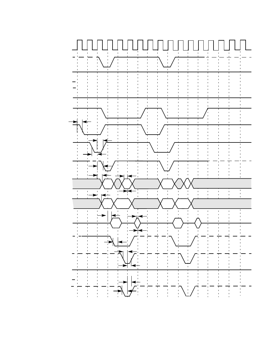
Figure 6.19 Back to Back Read, 32-Bit Address and Data
t
4
t
1
t
3
t
1
CLK
(Driven by System)
GPIO0_FETCH/
(Driven by LSI53C1000R)
GPIO1_MASTER/
(Driven by LSI53C1000R)
REQ/
(Driven by LSI53C1000R)
PAR
(Driven by LSI53C1000R-
IRDY/
(Driven by LSI53C1000R)
TRDY/
(Driven by Target)
STOP/
(Driven by Target)
DEVSEL/
(Driven by Target)
t
1
t
6
t
3
AD[31:0]
(Driven by LSI53C1000R-
C_BE[3:0]/
(Driven by LSI53C1000R)
t
3
CMD
t
2
REQ64/
(Driven by LSI53C1000R)
ACK64/
(Driven by LSI53C1000R)
t
1
t
2
GNT/
(Driven by Arbiter)
FRAME/
(Driven by LSI53C1000R)
t
5
Data
In
Addr
Out
Data
In
Addr
Out
CMD
t
3
t
2
t
2
Addr; Target-Data)
Addr; Target-Data)
t
3
BE
BE
Out
In
Out
In
Advertising
This manual is related to the following products: