New prod uc t zxbm5210 electrical characteristics, Zxbm5210 – Diodes ZXBM5210 User Manual
Page 4
ZXBM5210
Document number: DS36765 Rev. 1 - 2
4 of 17
December 2013
© Diodes Incorporated
NEW PROD
UC
T
ZXBM5210
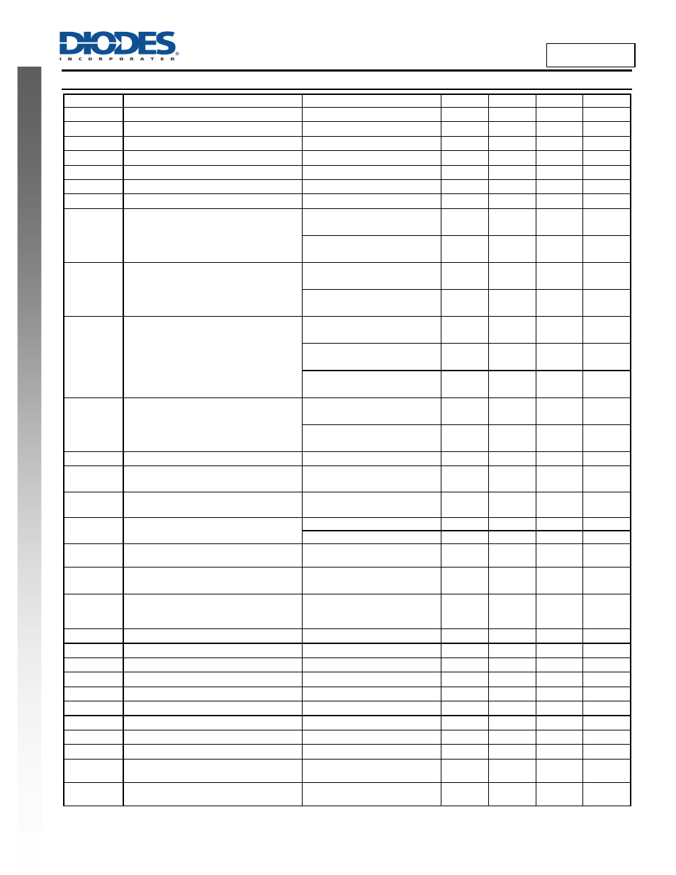
Electrical Characteristics
(Note 9)(@T
A
= +25°C, V
DD
= 12V, unless otherwise specified.)
Symbol Characteristics
Conditions
Min
Typ
Max
Unit
I
DD
Supply Current
No Load
—
0.85
2.5
mA
I
DD_STNDBY
Standby Supply Current
FWD=REV=LOW (GND)
—
32 45
uA
V
UV_TH
Under Voltage lock Out Threshold
Voltage Decreasing
—
2.6 — V
V
UVLO_R
Under Voltage Lock Out Release Threshold Voltage Increasing
—
2.8 3.0 V
V
UV_HYS
Under Voltage Hysteresis
Voltage Increasing
—
200 — mV
V
OV_TH
Overvoltage Threshold
Voltage Increasing
—
20.7 24 V
V
OV_RLTH
Overvoltage Release Threshold
Voltage Decreasing
17.0
19
—
V
V
OH
Output Voltage High
I
OUT
= 300mA,
T
A
= -
40
°C to +105°C
V
DD
- 0.25 V
DD
- 0.15
— V
I
OUT
=500mA
T
A
= -
40
°C to +105°C
V
DD
- 0.43 V
DD
- 0.25
— V
V
OL
Output Voltage Low
I
OUT
= 300mA,
T
A
= -
40
°C to +105°C
— 0.15
0.25 V
I
OUT
= 500mA,
T
A
= -
40
°C to +105°C
— 0.25
0.43 V
V
OH
+ V
OL
Output voltage of N- and PMOS and bond
wire voltage drop combined
I
OUT
= 300mA,
T
A
= -
40
°C to +105°C
— 0.3 0.5 V
I
OUT
= 500mA,
T
A
= -
40
°C to +105°C
— 0.5 0.86 V
I
OUT
= 300mA, V
DD
= 3V
T
A
= -
40
°C to +105°C
—
0.39 0.66 V
R
ON_Total
Combined N- and PMOS R
DSON
including
bond wire resistance
I
OUT
= 500mA,
T
A
= -
40
°C to +105°C
— 1
1.72
Ω
I
OUT
= 300mA, V
DD
= 3V
T
A
= -
40
°C to +105°C
— 1.3 2.2
Ω
I
LIM_TH
Over current protection threshold
1.2
1.5
A
V
REF
V
REF
voltage range
( DC voltage speed control mode)
3
—
V
DD
(18V max)
V
I
VREF
V
REF
bias current
( DC voltage speed control mode)
V
REF
= V
DD
-15 0 15 μA
F
OUT
Output PWM switching frequency
(Internal PWM oscillator)
VREF
control mode
20
26.5
35
kHz
PWM speed control mode
20
—
100 kHz
F
FWD_REV
Input PWM frequency of speed control
signal
PWM control mode
20
—
100
kHz
T
DEAD
Dead time between current reversal
V
DD
= 3V to 18V
T
A
= -
40
°C to +105°C
2.1 3 3.9 μs
t
SDN_DELAY
Shutdown delay – Internal circuits active
after FWD = REV = L
(except from brake mode)
FWD = GND
REV = GND
125 180 —
μs
V
FWDH
FWD Input H Level
2
—
5.5
V
V
FWDL
FWD Input L Level
0
—
0.8
V
I
FWDH
FWD pin current – H Level
FWD pin: V
FWD
= 5V
— 50 —
μ
A
I
FWDL
FWD pin current – L Level
FWD pin: V
FWD
= 0V
— 50 —
μ
A
V
REVH
REV Input H Level
2
—
5.5
V
V
REVL
REV Input L Level
0
—
0.8
V
I
REVH
REV pin current – H Level
REV pin: V
RVS
= 5V
— 50 —
μ
A
I
REVL
REV pin current – L Level
REV pin: V
RVS
= 0V
— 50 —
μ
A
D
PWM_MIN
Output minimum duty ratio
0%
100
%
Tj_
SDN_TH
IC junction temperature thermal shutdown
threshold
—
165
—
o
C
Tj_
SDN_HYST
IC junction temperature thermal shutdown
hysteresis
—
25
—
o
C
Note
:
9. Typical data is at T
A
= +25
°C, V
DD
= 12V. The maximum and minimum parameters values over the operating temperature range are not tested in
production, they are guaranteed by design, characterization and process control.