Altera Stratix II GX EP2SGX90 Transceiver Signal Integrity Development Board User Manual
Page 15
Altera Corporation
Reference Manual
2–5
May 2006
Stratix II GX EP2SGX90 Transceiver Signal Integrity Development Board
Board Components & Interfaces
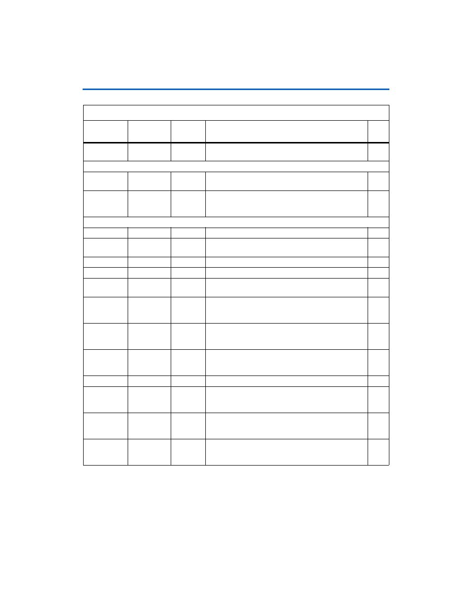
Display
Configuration
done LED
D14
LED that illuminates upon successful FPGA configuration.
Memory
Flash
16 Mbytes of
flash memory
U19
16 Mbytes of non-volatile memory.
Serial flash
64 Mbits of
serial flash
memory
U22
Altera
®
EPCS64 low-cost serial configuration device to
configure the Stratix II GX device
Clock Circuitry
Crystal
Clock
U6
Crystal 25MHz
Clock
Generator
Clock
U5
Spread spectrum clock generator for 25-MHz, 100-MHz,
125-MHz, and 200-MHz clocks.
Oscillator
Clock
U9
156.25-MHZ oscillator
Buffer
Clock
U8
1:4 differential fan-out buffer
Buffer
Clock
U7
Differential to single-ended converter for providing trigger
clocks.
Input
SMA external
clock input
connectors
J5, J6
SMA connectors for providing an external clock to the three
quad transceivers.
Output
SMA trigger
clock
connector
J3
SMA connector for the PCIe trigger clock.
Output
SMA trigger
clock
connector
J4
SMA connector for the basic trigger clock associated with
the three quad transceivers.
Oscillator
Clock
U10
50-MHz clock oscillator used for the system clock.
Input
SMA input
clock
connectors
J7, J8
Reference clock input for quad 1 transceiver
Input
SMA input
clock
connectors
J9, J10
Reference clock input for quad 3 transceiver
Output
SMA output
clock
connectors
J12, J14
Output clock from Stratix II GX
Table 2–1. Stratix II GX Transceiver SI Development Board Components & Interfaces (Part 2 of 3)
Type
Component/
Interface
Board
Reference
Description
Page