Altera Stratix II GX EP2SGX90 Transceiver Signal Integrity Development Board User Manual
Page 21
Altera Corporation
Reference Manual
2–11
May 2006
Stratix II GX EP2SGX90 Transceiver Signal Integrity Development Board
Board Components & Interfaces
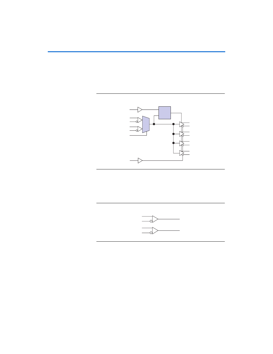
ICS8543 (U8): General Purpose 1:4 Differential Fanout Buffer
The ICS8543 is a general purpose clock buffer with a 2:1 multiplexer input
and a 1:4 differential fanout. The clk_sel signal determines which clock
input (i.e., clk or pclk) is used; the chosen signal is then converted to
four output clocks. See
Figure 2–4. ICS8543 Clock Buffer Block Diagram
ICS83023 (U7): Differential I/O to Single Converter for Trigger Clock
The ICS83023 is a differential I/O to a single-ended clock buffer, which is
used for both the PCI-Express and Basic trigger clocks. See
Figure 2–5. ICS83023 Clock Buffer Block Diagram
D
0
1
Q
LE
clk_en
clk
nclk
pclk
npclk
clk_sel
oe
Q0
nQ0
Q1
nQ1
Q2
nQ2
Q3
nQ3
clk0
nclk0
clk1
nclk1
Q0
Q1