Dip switches (s7 and s8), Dip switches (s7 and s8) -22 – Altera Stratix II GX EP2SGX90 Transceiver Signal Integrity Development Board User Manual
Page 32
2–22
Reference Manual
Altera Corporation
Stratix II GX EP2SGX90 Transceiver Signal Integrity Development Board
May 2006
Interfaces
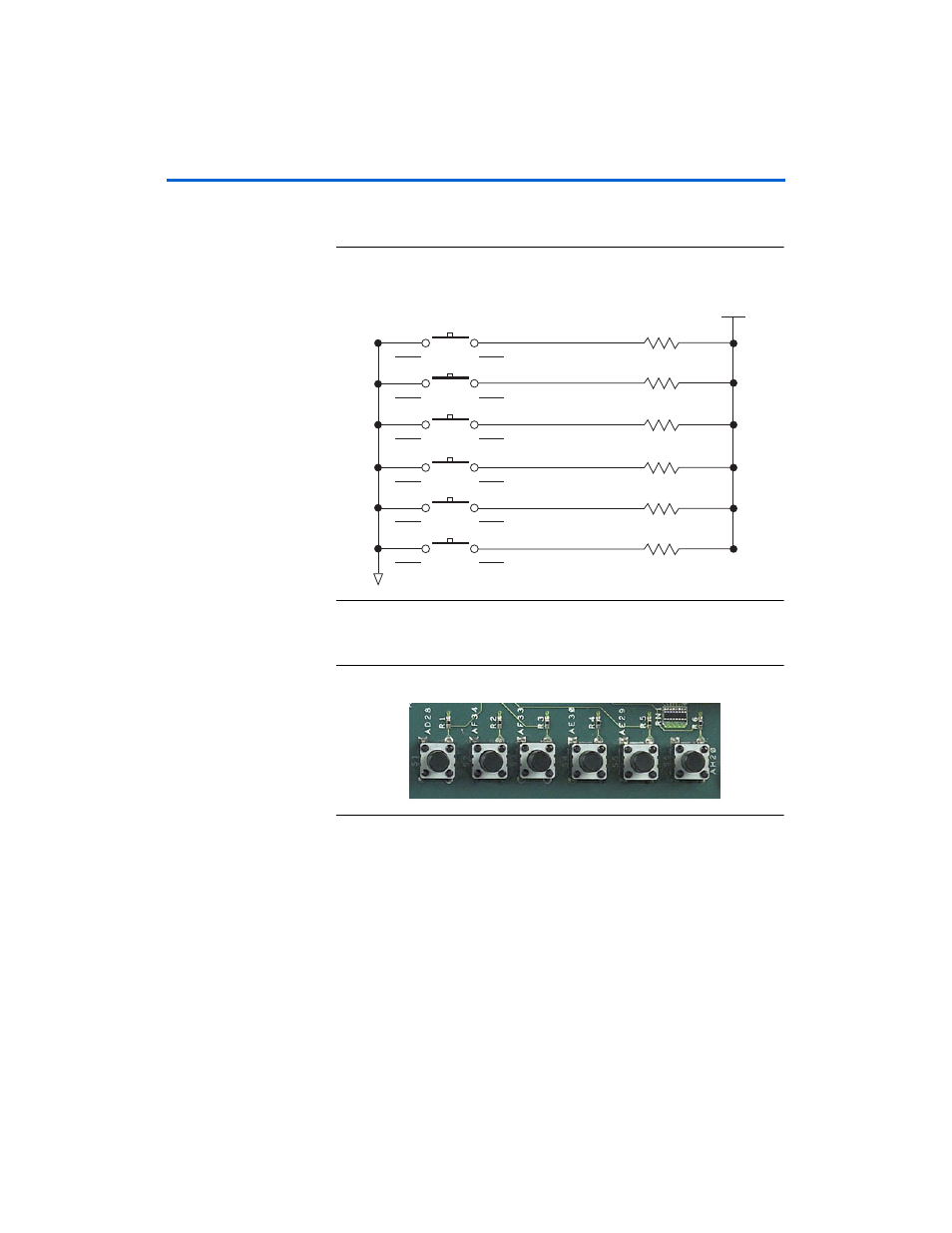
shows the push-button switch circuitry.
Figure 2–13. Push-Button Switch Circuitry
shows the push-button board image.
Figure 2–14. Push-Button Board Image
DIP Switches (S7 and S8)
Board references S7 and S8 are banks of six DIP switches. The DIP
switches in S7 are user-defined, and DIP switches in S8 control the PCIe
clock speed, PCIe clock spread spectrum setting, and the output enable of
the clocks to the three quad transceivers. In the open position, the selected
signal is driven to logic 1. In the closed position, the selected signal is
driven to logic 0.
3
V
3
A
B
A2
B2
PB0_I
N
P
u
sh-B
u
tton S
w
itch Circ
u
itry
S1
R1
1K
A
B
A2
B2
S2
A
B
A2
B2
S3
A
B
A2
B2
S4
A
B
A2
B2
S5
A
B
A2
B2
S6
PB1_I
N
R2
1K
PB2_I
N
R3
1K
PB3_I
N
R4
1K
PB3_I
N
R5
1K
PB5_I
N
R6
1K