Altera Stratix II GX EP2SGX90 Transceiver Signal Integrity Development Board User Manual
Page 27
Advertising
Altera Corporation
Reference Manual
2–17
May 2006
Stratix II GX EP2SGX90 Transceiver Signal Integrity Development Board
Board Components & Interfaces
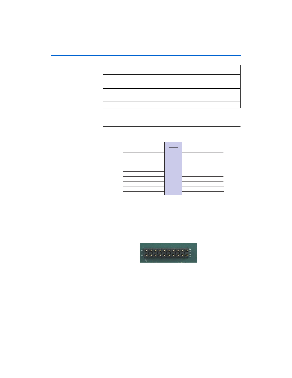
shows the debug header’s schematic.
Figure 2–8. Debug Header (J1) Schematic
Figure 2–9
shows the debug header’s board labels.
Figure 2–9. Debug Header (J1) Board Labels
18
D_HED17
AB26
19
D_HED18
AB25
20
D_HED19
AD32
Table 2–10. Debug Header Pin-Out (Part 2 of 2)
Header Number
Schematic Signal Name
Stratix II GX (U20)
Pin Number
D_HED0
D_HED2
D_HED4
D_HED6
D_HED
8
D_HED10
D_HED12
D_HED14
1
3
5
7
9
11
2
4
6
8
10
12
13
14
15
16
J1
De
bu
g
Header
D_HED16
D_HED1
8
D_HED1
D_HED3
D_HED5
D_HED7
D_HED9
D_HED11
D_HED13
D_HED15
D_HED17
D_HED19
17
1
8
19
20
CO
NN
_PCB_10X2
Advertising