Clock structure, 1 overview, Table 5-1 – Artesyn COMX-P40x0 ENP2 Installation and Use (August 2014) User Manual
Page 79: Figure 5-1, Clock distribution, Chapter 5
Chapter 5
COMX-P40x0 ENP2 Installation and Use (6806800R95B)
79
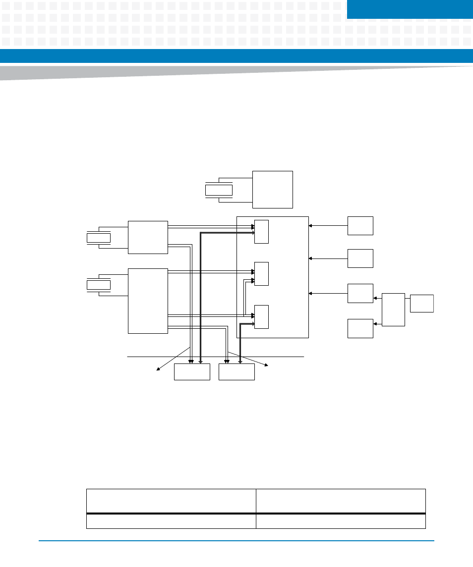
Clock Structure
5.1
Overview
The COMX-P40x0 ENP2 needs several kinds of single ended and differential clocks for booting
up and normal operating. Following is the clock distribution tree:
The output frequency of the bank 1 and bank 2/3 SERDES clocks is selectable between
100MHz and 125MHz. This must be set correctly by the carrier or corresponding CPU GPIO
pins depending on what RCW SERDES configuration is selected. For proper settings, refer
Figure 5-1
Clock Distribution
Table 5-1 Configuration of the frequency of SERDES reference clock by carrier
SERDES bank 1 reference clock select (pin B97
on COME)
SERDES bank 2/3 reference clock select (pin B98
on COME)
Bank1_SEL_FS0=0, 100MHz
Bank2_SEL_S1=0, 100MHz
Bank 1
Bank 2
Bank 3
GE PHY
Crystal
ICS9FG104
(<50ps)
Crystal
ICS9FG104
(<50ps)
Crystal
100 MHz
OSC
RTC
32.768 KHz
24 MHz
OSC
USB
PHY
Device on
Carrier
COME Connector
100 MHz
100 MHz
125 MHz
USB
PHY
CY2305
Device on
Carrier
125 MHz
P40x0
100 MHz
32.768 KHz
60 MHz
24 MHz
Reference clock for
Bank 2#/3#
Reference clock
for Bank 1#