Fluke Biomedical 875 Victoreen User Manual
Page 26
Function Description
Readout Module876A-1
4
4-5
low ALERT ALARM jumper connected to the collector (pin 1) of the alert alarm relay driver
. The following options are available with the presence or absence of the jumper when the
AE/RESET indicator push button on the panel is depressed. This action occurs with
tomatic Reset - The alarm will continue to be activated only as long as the radiation exceeds the
Fail/Safe Circuit
stem.
the collector of Q502 is
cted,
device and the 876A-1 Readout Module output. Inputs to
as voltage dividers for the output. Their values for standard usage and available
he
t
202 on the ECS board and is activated by a muting voltage
There is a yel
stage of U503
radiation level exceeds the threshold and triggers the alarm:
Manual Reset - The alarm will continue to be activated even after the radiation level recedes below
threshold until the S
the jumper in place.
Au
threshold level. This action occurs with the jumper removed.
The yellow warning light acts similarly to the alarms. It lights when the alarm relay is de-energized.
Each relay contains four Form C contacts, but only two of them are accessible from the rear connector.
The connection to the yellow panel warning light is from terminal 2 of the printed circuit board, which is
connected to the collector (pin 14) of U503 through R526.
Input to the fail/safe circuit comes from pin 1 of U2 on the power supply board, entering the relay driver
board on pin H of the relay driver printed circuit board. The input is a DC voltage that is either high (15 V)
or low (0 V); if it is low, relay K3 is energized (non-alarm condition). If the signal is high, the green
SAFE/RESET lamp will go off and the relay is de-energized, indicating a fault somewhere in the sy
The circuit consists basically of two inverters in tandem so the voltage on
approximately the same as the input voltage, the diode CR508 preventing current flow through the
solenoid if the collector is slightly higher than the 14 V at the other end of the solenoid coil.
Recorders and Computer Buffers
Provisions have been made for delivering DC output voltages to a recorder and computer for further
processing. The buffers are located on the relay driver board. If a commercial device is to be conne
a signal isolator must be installed between the
both computer and recorder buffers arrive at pin R of the relay driver printed circuit board, coming from
terminal 3 on the ECS printed circuit board. The computer buffer consists of and OP AMP using pins 1, 2
and 3 of U501, the output being taken off the relay driver board at pins 4 (+) and 2 (-) of P502. Resistors
R532 and R533 act
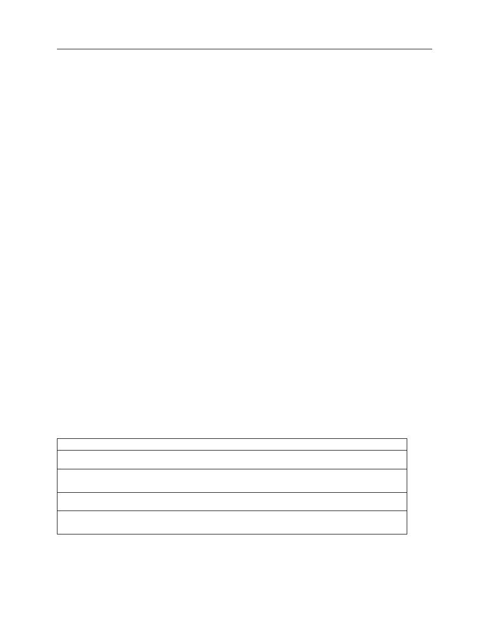
options are shown in Table 4-1.
The recorder buffer consists of an OP AMP using pins 5, 6 and 7 of U501, the output being taken off the
relay driver board at pins 1 (+) and 3 (-) of P502. Resistors R530 and R531 act as voltage dividers for t
output. Their value for standard usage and available options are shown in Table 4-1. Both buffers are
disabled during the ECS test by a switching circuit on the ECS board, so that the ECS current is no
recorded. This circuit consists of Q201 and Q
during the ECS test.
Table 4-1. Resistance Options for Voltage Dividers
Resistor
Std.
Option 1
Option 2
Option 3
Recorder
0 – 1 V
0
Voltage
– 10 mV
0 – 5 V
0 – 5V
R53
200 ohms
0
1 kilohm
119.8 kilohms
200 ohms
R53
200 ohms
1 kilohm
1 kilohm
1
200 ohms
Computer
Voltage
0 – 5 V
1 – 100 mV
0 – 50 mV
0 – 5 V
R53
0 ohms
2
200 ohms
11.8 kilohms
23.8 kilohms
20
R53
s
200 ohms
1 kilohm
3
1 kilohm
200 ohm