Factory default switch settings, Factory default switch settings –2 – Altera Arria II GX FPGA User Manual
Page 16
4–2
Chapter 4: Development Board Setup
Factory Default Switch Settings
Arria II GX FPGA Development Kit User Guide
February 2011
Altera Corporation
Factory Default Switch Settings
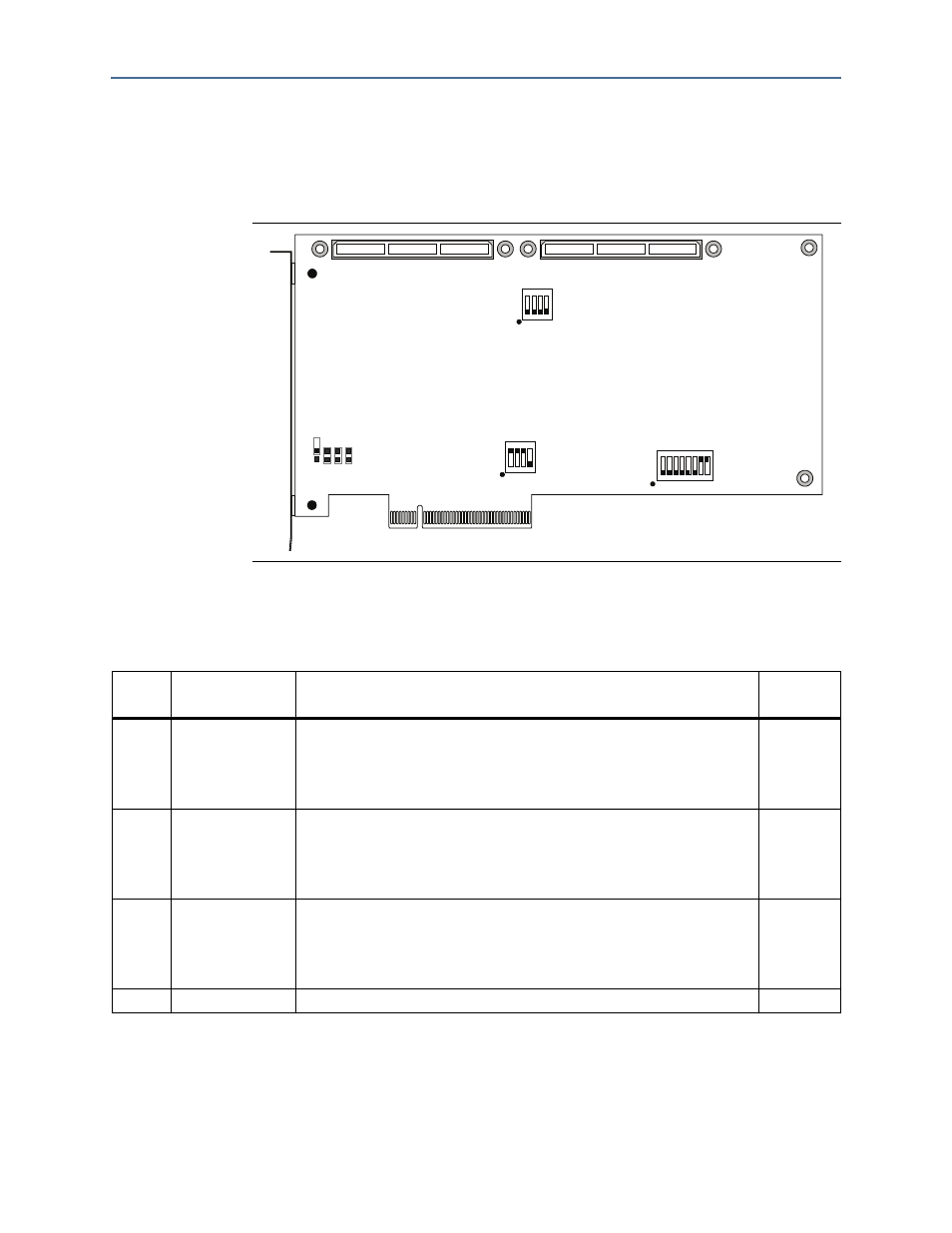
This section shows the factory switch settings for the Arria II GX FPGA development
board.
shows the switch locations and the default position of each switch.
To restore the switches to their factory default settings, perform the following steps:
1. Set DIP switch bank (SW3) to match
and
Figure 4–1. Switch Locations and Default Settings on the FPGA Development Board
SW4
1 2 3 4 5 6 7 8
ON
Board Settings
DIP Switch
ON = 0
OFF = 1
4
3
2
1
SW2
ON
User
DIP Switch
ON = 0
OFF = 1
4
3
2
1
SW3
ON
PCIe MODE
DIP Switch
(in
stalled
)
(in
stalled
)
(in
stalled
)
(n
o
t in
stalled
)
J9
JTAG Control
Jumpers
Table 4–1. SW3 Dip Switch Settings
Switch
Board
Label
Function
Default
Position
1
PCIe x1
Switch 1 has the following options:
■
When off, the PCIe card PCIE_PRSNT2n_x1 signal is connected to PCIe
card PRSNT1 signal.
■
When on, the PCIe card PCIE_PRSNT2n_x1 signal floats.
On
2
PCIe x4
Switch 2 has the following options:
■
When off, the PCIe card PCIE_PRSNT2n_x4 signal is connected to PCIe
card PRSNT1 signal.
■
When on, the PCIe card PCIE_PRSNT2n_x4 signal floats.
On
3
PCIe x8
Switch 3 has the following options:
■
When off, the PCIe card PCIE_PRSNT2n_x8 signal is connected to PCIe
card PRSNT1 signal.
■
When on, the PCIe card PCIE_PRSNT2n_x8 signal floats.
On
4
—
■
—
—