Preparing design files for flash programming, Creating flash files using the nios ii eds – Altera Arria II GX FPGA User Manual
Page 42
A–2
Appendix A
Preparing Design Files for Flash Programming
Arria II GX FPGA Development Kit User Guide
February 2011
Altera Corporation
c
Altera recommends that you do not overwrite the factory hardware and factory
software images unless you are an expert with the Altera tools. If you unintentionally
overwrite the factory hardware or factory software image, refer to
Flash Device to the Factory Settings” on page A–4
.
Preparing Design Files for Flash Programming
You can obtain designs containing prepared .flash files from the
page of the Altera website or create .flash files from your own
custom design.
The Nios II EDS sof2flash command line utility converts your Quartus II-compiled
.sof
into the .flash format necessary for the flash device. Similarly, the Nios II EDS
elf2flash
command line utility converts your compiled and linked Executable and
Linking Format File (.elf) software design to .flash. After your design files are in the
.flash
format, use the Board Update Portal or the Nios II EDS
nios2-flash-programmer
utility to write the .flash files to the user hardware 1 and
user software locations of the flash memory.
f
For more information about Nios II EDS software tools and practices, refer to the
page of the Altera website.
Creating Flash Files Using the Nios II EDS
If you have an FPGA design developed using the Quartus II software, and software
developed using the Nios II EDS, follow these instructions:
1. On the Windows Start menu, click All Programs > Altera > Nios II EDS > Nios II
Command Shell
.
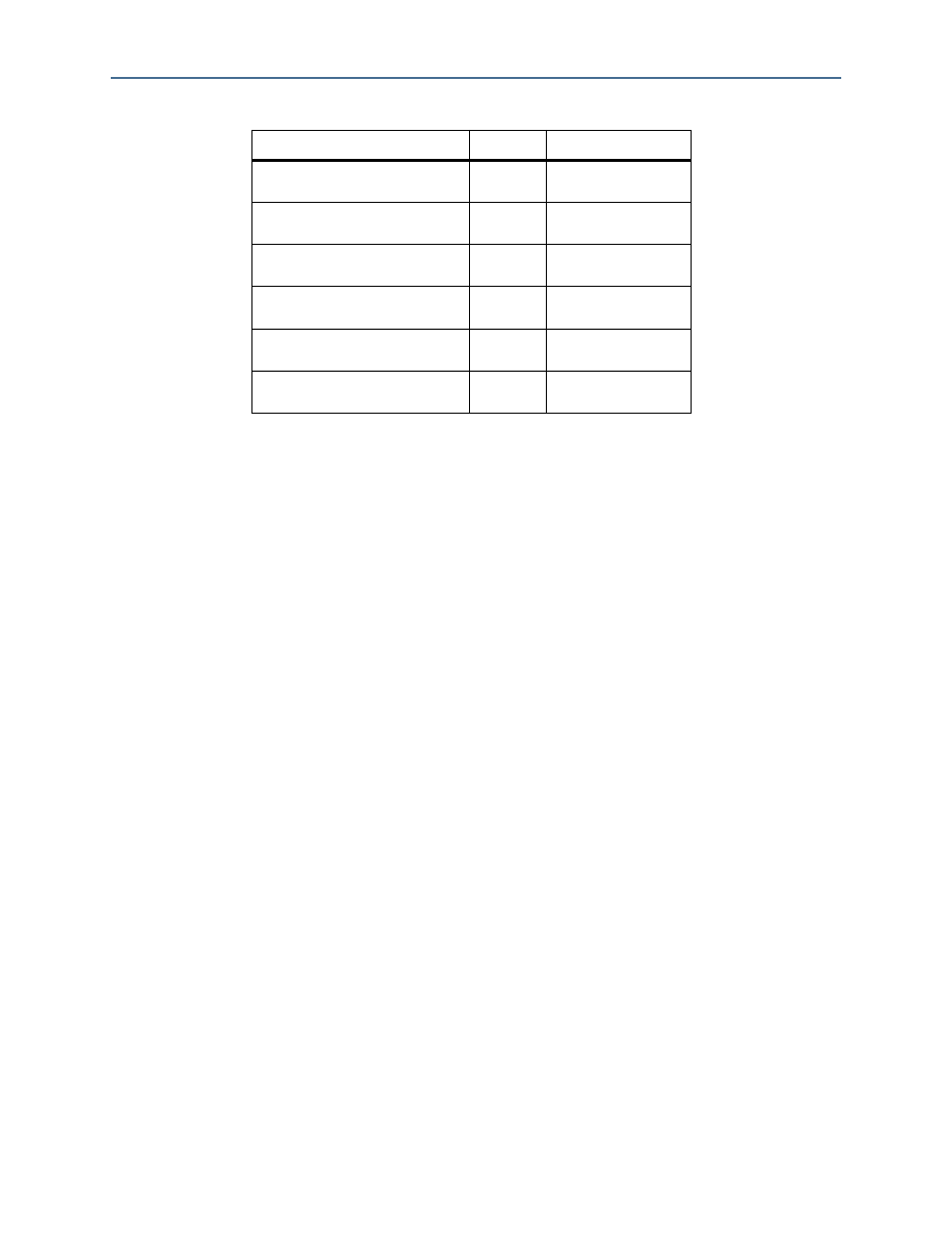
User hardware 1
6,357 KB
0x00C5FFFF
0x00640000
Factory hardware
6,357 KB
0x0063FFFF
0x00020000
PFL option bits
32 KB
0x0001FFFF
0x00018000
Board information
32 KB
0x00017FFF
0x00010000
Ethernet option bits
32 KB
0x0000FFFF
0x00008000
User design reset vector
32 KB
0x00007FFF
0x00000000
Table A–1. Byte Address Flash Memory Map (Part 2 of 2)
Block Description
Size
Address Range