Altera Arria II GX FPGA User Manual
Page 17
Chapter 4: Development Board Setup
4–3
Factory Default Switch Settings
February 2011
Altera Corporation
Arria II GX FPGA Development Kit User Guide
2. Set DIP switch bank (SW4) to match
and
3. Set the board jumpers to match
and
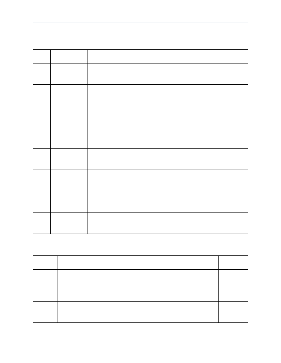
Table 4–2. SW4 Dip Switch Settings
Switch
Board
Label
Function
Default
Position
1
DIP0
Switch 1 has the following options:
■
When on, reserved.
■
When off, reserved.
Off
2
DIP1
Switch 2 has the following options:
■
When on, reserved.
■
When off, reserved.
Off
3
DIP2
Switch 3 has the following options:
■
When on, reserved.
■
When off, reserved.
Off
4
USER LOAD
Switch 4 has the following options:
■
When on, the PFL loads the user hardware 1 design on power up.
■
When off, the PFL loads the factory design on power up.
Off
5
PWR MON
Switch 5 has the following options:
■
When on, reserved.
■
When off, reserved.
Off
6
USB DISn
Switch 6 has the following options:
■
When on, reserved.
■
When off, reserved.
Off
7
CLK EN
Switch 7 has the following options:
■
When on, all on-board oscillators are enabled.
■
When off, on-board oscillators to the FPGA are disabled.
On
8
CLK SEL
Switch 8 has the following options:
■
When on, programmable oscillator clock (U30) is selected.
■
When off, LVPECL SMA clock (J10 and J11) is selected.
On
Table 4–3. JTAG Chain Jumper Settings (Part 1 of 2)
Board
Reference
Board
Label
Function
Default
Shunt Position
J9 pins 1-2
MAX DIS
This jumper has the following options:
■
Installing the shunt removes the MAX II EPM2210 device from the
JTAG chain.
■
Removing the shunt includes the MAX II EPM2210 device in the
JTAG chain.
Not installed
J9 pins 3-4
HSMA DIS
This jumper has the following options:
■
Installing the shunt removes HSMC port A from the JTAG chain.
■
Removing the shunt includes HSMC port A in the JTAG chain.
Installed