Clock enable signals, Single register clock enable circuit, Clock enable signals –4 – Altera Clock Control Block IP Core User Manual
Page 16: Single register clock enable circuit –4
3–4
Chapter 3: Functional Description
Clock Control Block
Clock Control Block (ALTCLKCTRL) Megafunction
February 2014
Altera Corporation
User Guide
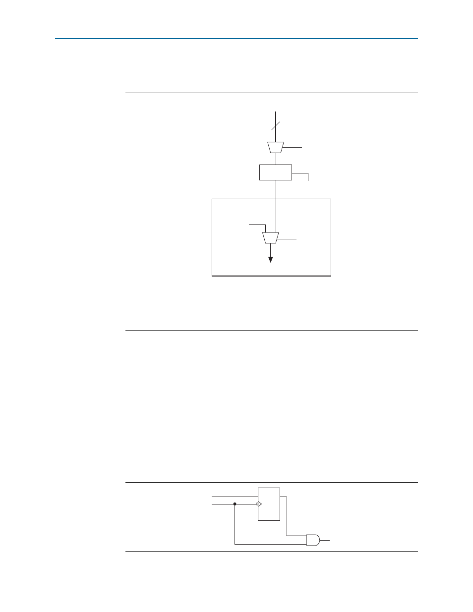
Figure 3–3
shows a clock control block configured to drive a dedicated external clock
out.
f
For more information about external PLL output clock control block or network in a
specific device, refer to the respective device handbook.
Clock Enable Signals
Single Register Clock Enable Circuit
In Cyclone III and Cyclone IV devices, the clock enable signals are supported at the
clock network level. This allows you to enable or disable the GCLK and RCLK
networks, or the PLL_OUT pins, which is useful for applications that require low power
or sleep mode.
shows how the ena clock enable signal is implemented.
Figure 3–3. External PLL Output Clock Control Block
(1)
Notes to
Figure 3–3
:
(1) The clock control block feeds to a multiplexer within the PLL_OUT pin’s I/O element (IOE). The PLL_OUT pin is a dual-
purpose pin. Therefore, this multiplexer selects either an internal signal or the output of the clock control block.
(2) You can only set these clock select signals through the configuration file and cannot be dynamically controlled during
user-mode operation.
6
Internal Logic
Enable/
Disable
Internal Logic
Static Clock
Select
(1)
Static Clock
Select
(1)
PLL_Out Pin
PLL Counter Outputs
(c[0..5])
Figure 3–4. Clock Enable Implementation in Cyclone III and Cyclone IV Devices
D
Q
clkena
clk
clkena out
clk_out