Double register clock enable circuit, Clock enable timing, Connectivity restrictions – Altera Clock Control Block IP Core User Manual
Page 17: General restrictions, Double register clock enable circuit –5, Clock enable timing –5, Connectivity restrictions –5, General restrictions –5
Chapter 3: Functional Description
3–5
Connectivity Restrictions
February 2014
Altera Corporation
Clock Control Block (ALTCLKCTRL) Megafunction
User Guide
1
Single register is applicable for Cyclone III and Cyclone IV devices only.
f
For more information about clock enable signals in a specific device, refer to the
respective device handbook.
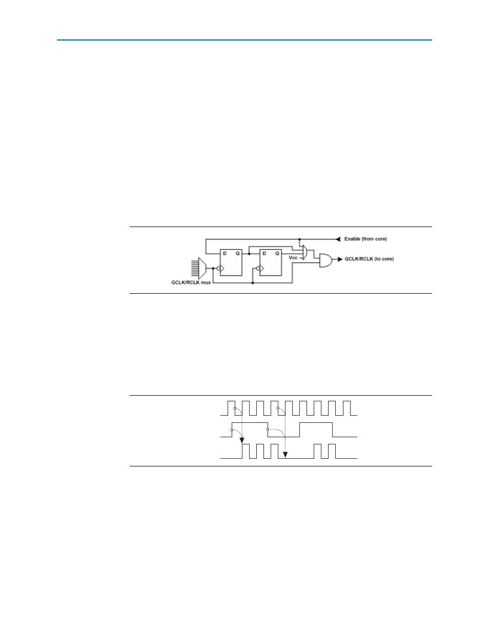
Double Register Clock Enable Circuit
The double register clock enable circuit in Arria V, Arria 10, Cyclone V, Stratix III and
Stratix IV devices helps with asynchronous enable/disable of the clock network, and
avoid metastability issues. If the enable signal can toggle at any time, it’s possible that
if the enable toggles at the same instant as the falling clock edge, the register can get
“stuck” in a state between 0 and 1 for some time, before resolving. Having two
registers on the path acts as a synchronization chain and reduces the probability of
getting stuck in this state.
shows the double register clock enable circuit.
f
For more information about metastability issues, refer to
chapter of the Quartus II Handbook.
Clock Enable Timing
Figure 3–6
shows a functional timing waveform example for clock-output enable.
Clock enable is synchronous with the falling edge of the input clock.
Connectivity Restrictions
The following section describes the restrictions associated with the signal sources that
can drive the inclk[] input.
General Restrictions
■
The inclk[] ports that you use must be consistent with the clkselect[] ports that
you use.
Figure 3–5. Double Register Clock Enable Circuit
Figure 3–6. Clock Enable Timing
inclk
ena
outclk