Factory default switch settings, Figure 4–1, Shows – Altera Cyclone III LS FPGA User Manual
Page 14
4–2
Chapter 4: Development Board Setup
Factory Default Switch Settings
Cyclone III LS FPGA Development Kit User Guide
© October 2009 Altera Corporation
Factory Default Switch Settings
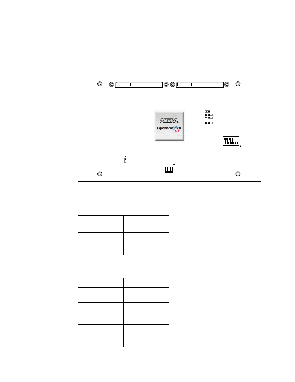
This section shows the factory switch settings for the Cyclone III LS FPGA
development board.
shows the switch bank locations and the default
position of each switch.
To restore the switches to their factory default settings, perform the following steps:
1. Set DIP switch bank (S7) to match
.
2. Set DIP switch bank (SW2) to match
Figure 4–1. Switch Locations and Default Settings on the FPGA Development Board
Table 4–1. S7 Dip Switch Settings
Switch
Position
1
On
2
On
3
On
4
On
Table 4–2. SW2 Dip Switch Settings
Switch
Position
1
On
2
On
3
On
4
On
5
Off
6
On
7
Off
8
Off
SW2
Board Settings
DIP Switch
OFF = 1
ON = 0
S7
User
DIP Switch
OFF = 1
ON = 0
J11
JTAG Control Jumpers
12
34
56
78
O P
EN
J12
4
3
2
1
O N
(not installed)
J18
LCD SEL
E P3CLS200F780
(not installed)
(not installed)
(not installed)
(installed)