Altera Cyclone III LS FPGA User Manual
Page 20
6–2
Chapter 6: Board Test System
Introduction
Cyclone III LS FPGA Development Kit User Guide
© October 2009 Altera Corporation
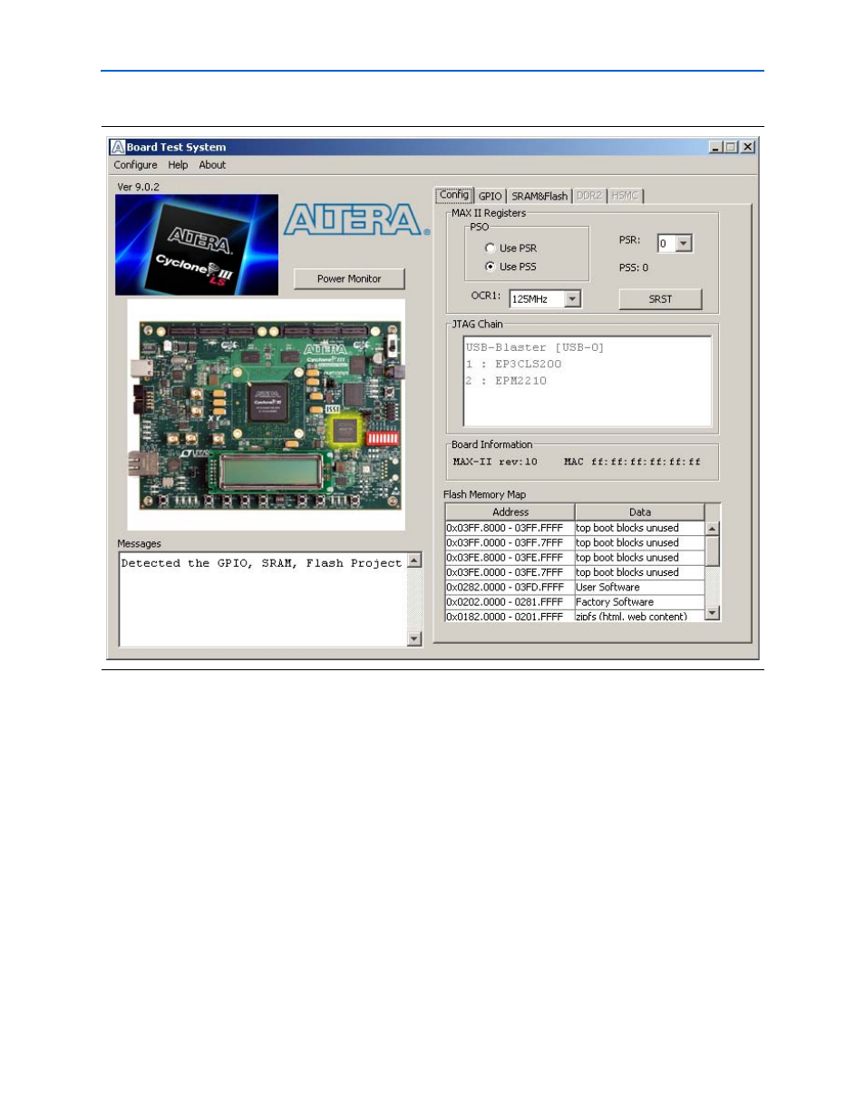
Several designs are provided to test the major board features. Each design provides
data for one or more tabs in the application. The Configure menu identifies the
appropriate design to download to the FPGA for each tab.
After successful FPGA configuration, the appropriate tab appears and allows you to
exercise the related board features. Highlights appear in the board picture around the
corresponding components.
The Power Monitor button starts the Power Monitor application that measures and
reports current power information for the board. Because the application
communicates over the JTAG bus to the MAX II device, you can measure the power of
any design in the FPGA, including your own designs.
1
The Board Test System and Power Monitor share the JTAG bus with other
applications like the Nios II debugger and the SignalTap
®
II Embedded Logic
Analyzer. Because the Quartus II programmer uses most of the bandwidth of the
JTAG bus, other applications using the JTAG bus might time out. Be sure to close the
other applications before attempting to reconfigure the FPGA using the Quartus II
Programmer.
Figure 6–1. Board Test System Graphical User Interface