The sram&flash tab – Altera Cyclone III LS FPGA User Manual
Page 26
6–8
Chapter 6: Board Test System
Using the Board Test System
Cyclone III LS FPGA Development Kit User Guide
© October 2009 Altera Corporation
Pushbutton Switches
This read-only control displays the current state of the board user push buttons. Press
a push button on the board to see the graphical display change accordingly.
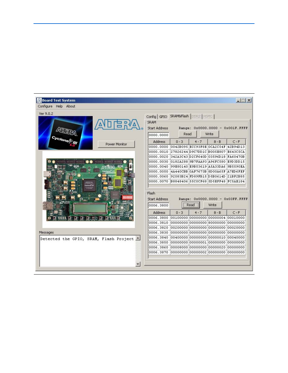
The SRAM&Flash Tab
The SRAM&Flash tab allows you to read and write SRAM and flash memory on your
board.
shows the SRAM&Flash tab.
The following sections describe the controls on the SRAM&Flash tab.
SRAM
This control allows you to read and write the SRAM on your board. Type a starting
address in the text box and click Read. Values starting at the specified address appear
in the table.The base address of SRAM in this Nios II-based BTS design is
0x0D00.0000. The valid address range within the 2-MByte SRAM is 0x0000.0000
through 0x001F.FFFF, as shown in the GUI.
Figure 6–4. The SRAM&Flash Tab