Pre-defined test designs, Pre-defined test design results -10 – Altera Transceiver SI User Manual
Page 18
2–10
Getting Started User Guide
Altera Corporation
Transceiver Signal Integrity Development Kit, Stratix II GX Edition
June 2006
Test the Transceiver Performance Using Pre-Defined Designs
Test the
Transceiver
Performance
Using
Pre-Defined
Designs
The kit provides pre-defined test designs and an easy-to-use demo
application with a custom graphical user interface (GUI). The demo
application’s GUI allows extensive transceiver channel testing at various
data rates and clocking schemes.
This section provides:
■
Pre-defined test design results
■
Demo application GUI tutorial
Pre-Defined Test Designs
Altera engineers created a set of pre-defined test designs for you to
evaluate Stratix II GX device transceiver performance and board features.
As you can tell from the data listed in
Table 2–3
, the results can vary
dramatically when choosing from various clocking schemes and data
rates.
Table 2–3
lists the default transceiver settings.
f
Refer to the section
“Connect the Cables to the Board and Computer” on
for information on using the JTAG interface when configuring
the Stratix II GX device with one of the pre-defined designs. The
CONF DONE LED (D14) illuminates upon successful device
configuration. Also, the 7-segment display shows the programmed
SOF/POF number. For example, for the gxbguictrl_top1.sof the
7-segment display indicates the SOF with 01, and with the
gxbguictrl_top2.sof
the 7-segment display indicates the SOF with 02.
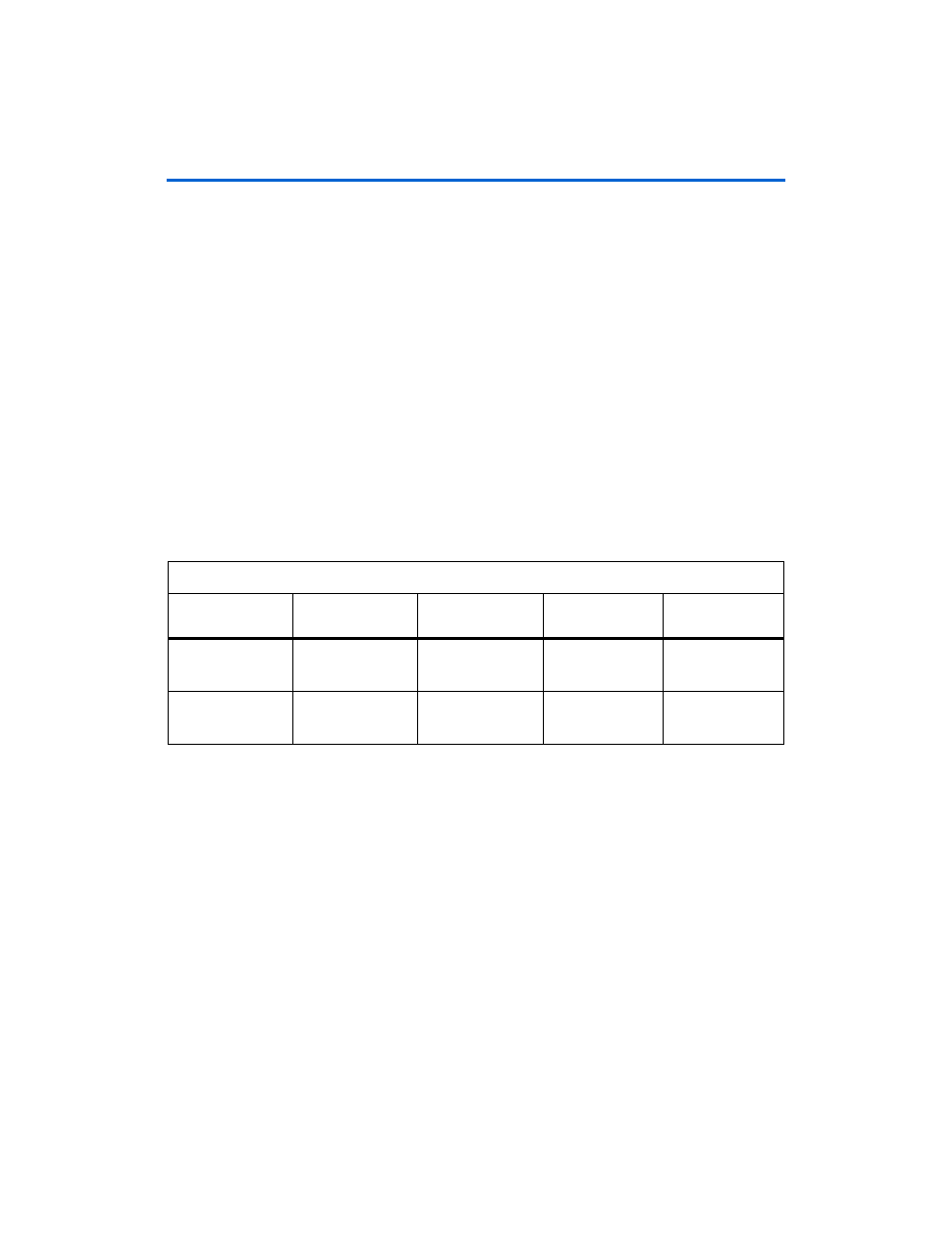
Table 2–3. Transceiver Test Design Results
File Name
Quad 1 Channel 1
Data Rate (Gbps)
Quad 2 Channel 1
Data Rate (Gbps)
Quad 3 Channel 1
Data Rate (Gbps)
Clocking Scheme
gxbguictrl_top1.sof 6.25
3.125
6.25
Clock from
156.25-MHz
oscillator
gxbguictrl_top2.sof 5
2.5
5
Clock from
156.25-MHz
oscillator
Note to
Table 2–3
:
(1)
The clock input can also be given from an external source. The frequency of the clock should be selected such that
the data rate in Quads 1 and 3 should be within the 6.375 Gbps - 3.126 Gbps range. For Quad2 the data rate should
be within the 3.125 Gbps-622 Mbps range. See
Table 2–4
.