Appendix a. non-gui based example design, Design features – Altera Transceiver SI User Manual
Page 29
Altera Corporation
Getting Started User Guide
A–1
June 2006
Transceiver Signal Integrity Development Kit, Stratix II GX Edition
Appendix A. Non-GUI Based
Example Design
Design Features
This manually-controlled (non-GUI based) example is a one channel
design using the microstrip transceiver quad at 6.25 Gbps. The input
clock frequency is 156.25 MHz and the interface is 40 bits wide. The
TX_P0
is connected to A4 and RX_P0 to C1. The other transceiver quads
that are not used are powered off. Data patterns supported are PRBS23,
PRBS7, and the high frequency pattern (1010).
1
The checkers are only available for the PRBS23 and PRBS7 data
patterns.
The following parameters can be controlled during run-time:
■
Preemphasis—Main tap (The other tap controls are not available.)
■
Equalization
■
DC gain
■
VOD
■
Data pattern select
■
Serial loopback
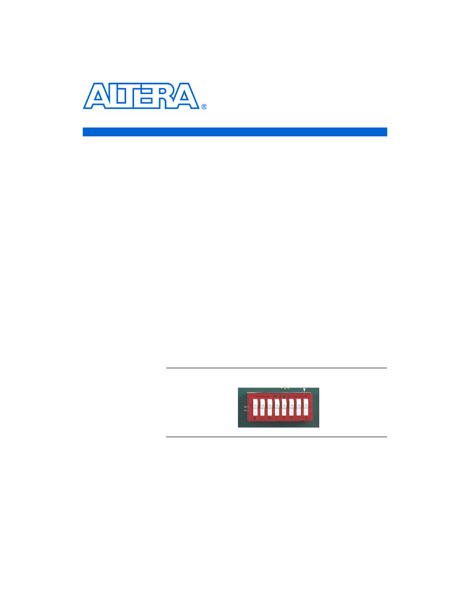
The parameters are controlled using a combination of DIP switches and
push-button switches. See
Table A–1
. The on-board frequency rate used
for the design is 156.25 MHz. Please set switch 6 in the clock setting DIP
switch bank (S8) to OPEN.
shows all the switches in the closed
position.
Figure A–1. Clock Setting DIP Switch Bank (All Switches In Closed Position)