Network loop timing, Network loop timing -5, Higher frequency) being converted to f – Verilink DIU 2130 (880-503297-001) Product Manual User Manual
Page 85
DIU/DIM Details
Verilink
7-5
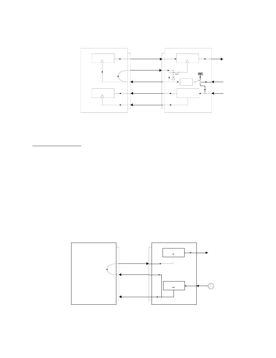
Figure 7-8 Source of Send Timing (ST)
ST controls the exact bit rate at which data is transmitted toward
the network on the DTE interface.
Network Loop
Timing
In loop timing, the received T1 signal generates both the RT and ST
signals. The receive T1 signal is the clock source. Figure 7-9 shows
the timing signal paths as follows:
•
The receive T1 signal clock is extracted in the CSU clock
recovery circuit. The clock is converted from T1 frequency
(1.544 Mbit/s) to the lower RT frequency in the DIU. This is
shown in the clock recovery circuit as f
h
(higher frequency)
being converted to f
l
(lower frequency).
•
In loop timing, ST is synchronized with RT.
•
The T1 transmit frequency is derived from the T1 receive
signal; therefore, the T1 transmit frequency is identical to the
T1 receive frequency.
Figure 7-9 Loop Timing
INT
Input Buffer
Freq.
Clock Recover
RCV Buffer
XMT Buffer
Converter
TT
ST ST
EXT
Loop
SD
RD
TT
RT
ST
Customer
Equipment
(DTE)
DSU
(DCE)
T1 XMT
T1 RCV
Ext
Clock
Input
Input Buffer
f
I
f
h
Clock Recovery
f
h
f
l
T1 XMT Frequency
T1 RCV Frequency
T1 XMT Frequency = T1 RCV Frequency
TT
ST
RT
Customer
Equipment
(DTE)
DSU
(DCE)