Chapter 3, Board layout – Lanner LEC-7950 User Manual
Page 15
14
Board Layout
Chapter 3
Embedded and Industrial Computing
Front Panel Function Pin Header (FRONT1): It provides
LED signal and button function on the front panel.
Clear CMOS jumper (CMOS1): It is for clearing the CMOS
data.
To erase the CMOS data:
Turn off the computer and unplug the power cord.
Move the jumper cap from pins 1-2(default) to pins
1.
2-3. Keep the cap on pins 2-3 for about 5-10 seconds,
then move the cap back to pins 1-2.
Plug the power cord and turn on the computer.
2.
Enter BIOS setup to re-enter data.
3.
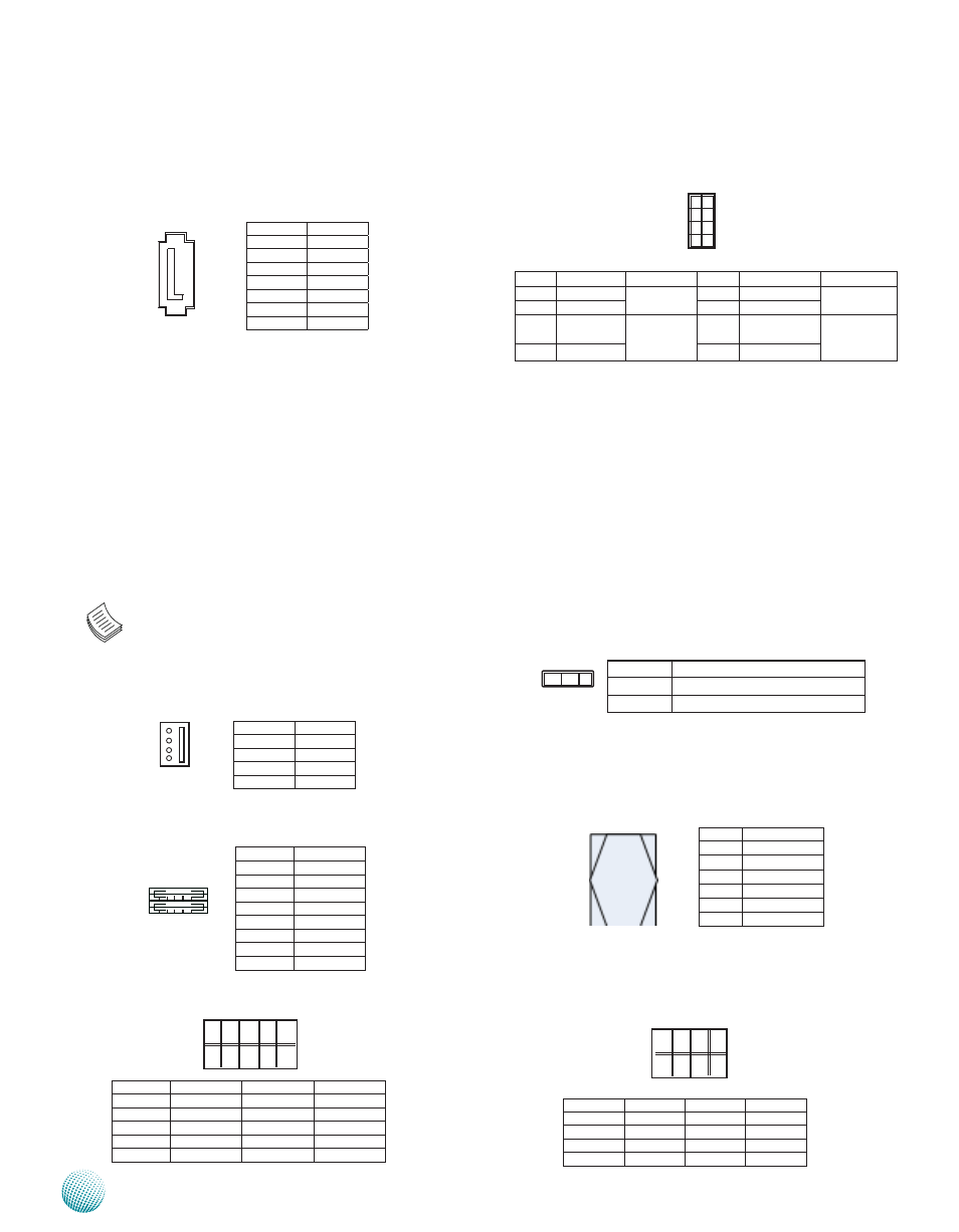
SIM Card Socket (SIM1):
Keyboard and Mouse Connector (KBM1)
Serial-ATA Connector (SATA1): It is for connecting a 2.5’’
hard disk to be served as your system’s storage. It can
support SATA II which features Data transfer rates up to
6.0 Gb/s (600 MB/s).
The controller contains two modes of operation—a
legacy mode using I/O space, and an AHCI mode using
memory space. software that uses legacy mode will not
have AHCI capabilities.
The AHCI ( Advanced Host Controller Interface) is a
programming interface which defines transactions
between the SATA controller and software and enables
advanced performance and usability with SATA. Platforms
supporting AHCI may take advantage of performance
features such as no master/slave designation for SATA
devices—each device is treated as a master—and
hardware assisted native command queuing. AHCI also
provides usability enhancements such as Hot-Plug.
Use the BIOS menu to configure your hard disk
to be AHCI compatible.
4-pin Serial-ATA Power Connector (SATA_PW1): It is for
connecting the SATA power cord.
Dual USB 2.0 Port Connector #0 and #1 (USB1)
Dual USB 2.0 Port Connector #2 and #3 (USB2)
Dual USB 2.0 Pin Header #4 and #5 (USB3)
1
3
5
7
2
4
6
8
Pin No.
description
C1
UIM_PWR
C2
UsIM_RsT
C3
UsIM_CLK
C5
GNd
C6
UsIM_VPP
C7
UsIM_dAT
C5 C7
C1 C3
1 2 3 4
5 6 7 8
Pin No.
Pin Name
1
UsB_VCC
2
UsBd0-
3
UsBd0+
4
GNd
5
UsB_VCC
6
UsBd1-
7
UsBd1+
8
GNd
Pin No.
Function
1
+12V
2
GNd
3
GNd
4
+5V
Pin No. Pin Name
Function
Pin No.
Pin Name
Function
1
Hd_LEd+
Hdd LEd
2
PWR_LEd+
Power LEd
3
Hdd_ACT#
4
PWR_LEd-
5
FP_RsT_
BTN_N
system Reset
Button
6
FP_PWR_
BTN_N
Power On/Off
Push Button
7
GNd
8
GNd
4
3
2
1
Pin No.
Pin Name
1-2
Normal (default)
2-3
Clear CMOs
3 2 1
Pin No.
Function
1
GNd
2
TX_P
3
TX_N
4
GNd
5
RX_N
6
RX_P
7
GNd
1
2
7
8
Pin No.
Function
Pin No.
Function
1
+5V
2
MsCLK
3
MsdATA
4
KEY
5
KBdATA
6
KEY
7
GNd
8
KBCLKs
Pin No.
Pin Name
Pin No.
Pin Name
1
UsB_VCC
2
3
UsBd4-
4
GNd
5
UsBd4+
6
UsBd5+
7
GNd
8
UsBd5-
10
UsB_VCC
10
9
2
1
1
2
3
4
5
6
7