Chapter 3, Board layout – Lanner LEC-7950 User Manual
Page 16
15
Board Layout
Chapter 3
Embedded and Industrial Computing
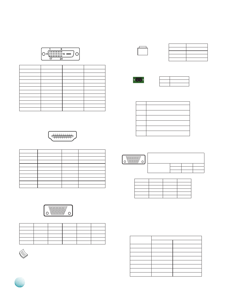
DVI-D Connector (DVID1): A single link DVI-D Connector
Pin No.
Description
Pin No.
Description
1
dATA_2N
2
dATA_2P
3
GNd
4
NC
5
NC
6
ddC_CLK
7
ddC_dAT
8
NC
9
dATA_1N
10
dATA_1P
11
GNd
12
NC
13
NC
14
+5V
15
GNd
16
HPd
17
dATA_0N
18
dATA_0P
19
GNd
20
NC
21
NC
22
GNd
23
CLK_P
24
CLK_N
HDMI Connector (HDMI1): An HDMI Connector
Pin No.
description
Pin No.
description
1
HdMI_dATP2_P
2
GNd
3
HdMI_dATP2_N
4
HdMI_dATP1_P
5
GNd
6
HdMI_dATP1_N
7
HdMI_dATP0_P
8
GNd
9
HdMI_dATP0_N
10
HdMI_CLK_P
11
GNd
12
HdMI_CLK_N
13
N/A
14
N/A
15
HdMI_ddC_CLK
16
HdMI_ddC_dAT
17
GNd
18
PHdMI
19
HdMI_HPd
VGA (VGA1)
Pin
signal
Pin
signal
Pin
signal
1
REd
6
CRT dET
11
N/A
2
GREEN
7
GNd
12
ddC dAT
3
BLUE
8
GNd
13
HsYNC
4
N/A
9
VCC5
14
VsYNC
5
GNd
10
GNd
15
ddC CLK
Note: The driver for the VGA and Audio ports
should be installed with the following order:
Chipset INF->Graphic->Audio
Reset Button (RST1)
Pin NO.
description
1
RsT_BTN
2
GNd
3
GNd
4
N/A
DC_IN CONNECTOR (CN1): A Phoenix connector for
external power supply.
Power Button (PBT1): Power button with dual LEDs
Digital Input/Output Connector (CN2): The 8 pins of
General Purpose Input/Output (GPIO) support input and
output operations through the DB-9 female connector.
LAN1/LAN2 Ports (LAN1/LAN2): The LAN ports are
provided by Intel 82574L Ethernet controller whose
interface complies with PCI-e 1.1 (2.5 Ghz). It has advanced
management features including IPMI pass-through via
SMBus or NC-SI, WOL, PXE remote boot, ISCSI boot and
VLAN filtering.
15 14 13 12 11
5 4 3 2 1
1
3
2
4
Pin No.
Pin Name
1
PWR_BTN_N
2
PWR_BTN_N
3
GNd
4
GNd
L1
PWR_sW_P
L2
PWR_sW_N
Pin No.
Description
Fast Ethernet Gigabit Ethernet
1
TX+
BI_DA+
2
TX-
BI_DA-
3
RX+
BI_DB+
4
--
BI_DC+
5
--
BI_DC-
6
RX-
BI_DB-
7
--
BI_DD+
8
--
BI_DD-
TTL Level is +5V; Maximum input current for
each port is 10mA; Maximum output current
for each port is 100uA
Input/Output
Voltage
Logic Register
0~2V
Low
0
2~5V
High
1
9 8 7 6
5 4 3 2 1
Pin No.
Pin Name
Pin No.
Pin Name
1
IN0
6
OUT0
2
IN1
7
OUT1
3
IN2
8
OUT2
4
IN3
9
OUT3
5
GNd
Pin No.
Pin Name
1
dC_GNd
2
dC_IN
1 2