Altera DSP Development Kit, Stratix V Edition User Manual
Page 44
2–36
Chapter 2: Board Components
Components and Interfaces
DSP Development Kit, Stratix V Edition
July 2012
Altera Corporation
Reference Manual
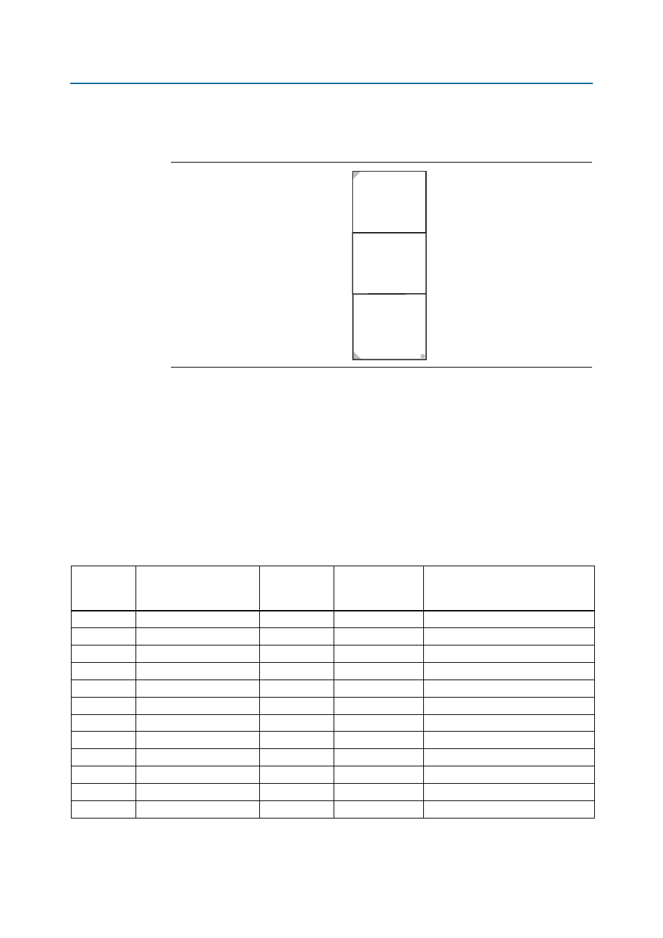
shows the bank arrangement of signals with respect to the Samtec
connector's three banks.
The HSMC interface has programmable bi-directional I/O pins that can be used as
2.5-V LVCMOS, which is 3.3-V LVTTL-compatible. You can also use these pins as
various differential I/O standards including, but not limited to, LVDS, mini-LVDS,
and RSDS with up to 17 full-duplex channels.
1
As noted in the
manual, LVDS and
single-ended I/O standards are only guaranteed to function when mixed according to
either the generic single-ended pin-out or generic differential pin-out.
lists the HSMC port A interface pin assignments, signal names, and
functions.
Figure 2–8. HSMC Signal and Bank Diagram
Bank 3
Power
D(79.40)
-or-
LVDS
CLKIN2, CLKOUT2
Bank 2
Power
D(39:0)
-or-
D[3:0] + LVDS
CLKIN1, CLKOUT1
Bank 1
8 TX Channels CDR
8 RX Channels CDR
JTAG
SMB
CLKIN0, CLKOUT0
Table 2–40. HSMC Port A Pin Assignments, Schematic Signal Names, and Functions (Part 1 of 4)
Board
Reference
(J1)
Schematic Signal Name
I/O Standard
Stratix V GS
Device Pin
Number
Description
40
HSMA_CLK_IN0
LVDS or 2.5-V
AG28
Primary single-ended clock in
98
HSMA_CLK_IN_N1
LVDS or 2.5-V
AT8
LVDS or CMOS clock in 1
158
HSMA_CLK_IN_N2
LVDS or 2.5-V
G6
LVDS or CMOS clock in 2
96
HSMA_CLK_IN_P1
LVDS or 2.5-V
AR8
Secondary differential clock in
156
HSMA_CLK_IN_P2
LVDS or 2.5-V
G7
Primary source-synchronous clock in
39
HSMA_CLK_OUT0
LVDS or 2.5-V
AJ10
Primary single-ended clock out
97
HSMA_CLK_OUT_N1
LVDS or 2.5-V
AH9
LVDS or CMOS clock out 1
157
HSMA_CLK_OUT_N2
LVDS or 2.5-V
G8
LVDS or CMOS clock out 2
95
HSMA_CLK_OUT_P1
LVDS or 2.5-V
AG9
Secondary differential clock out
155
HSMA_CLK_OUT_P2
LVDS or 2.5-V
G9
Primary source-synchronous clock out
30
HSMA_RX_P0
1.4-V PCML
AV2
Transceiver receive channel
32
HSMA_RX_N0
1.4-V PCML
AV1
Transceiver receive channel