Chapter 3, Board layout – Lanner LEC-2280 User Manual
Page 16
16
Board Layout
Chapter 3
Embedded and Industrial Computing
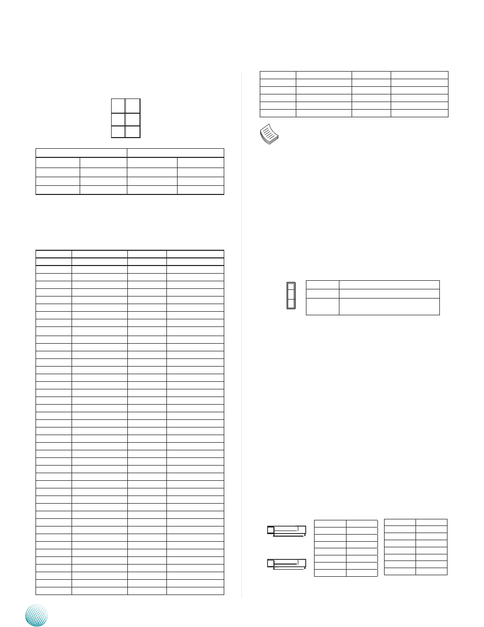
JP1, JP2: Select COM1 and COM2 Pin No9 (Ring Indicator)
function respectively
JP1
JP2
Pin
Signal
Pin
Signal
1-2
VCC5
1-2
VCC5
3-4
VCC12
3-4
VCC12
5-6
SPI_RI
5-6
SPI_RI
MIO1 on the expansion card: Connector for connecting
the COM port and audio expansion board to the LEC-2280
main board.
PIN
Pin Name
PIN
Pin Name
1
GNd
51
HdA_BCLK
2
N/A
52
HdA_sYNC
3
N/A
53
HdA_RsT
4
GNd
54
HdA_sdIN0
5
N/A
55
HdA_sdO
6
N/A
56
sPK
7
GNd
57
GNd
8
VCC5
58
VCC3
9
VCC5
59
VCC3
10
N/A
60
N/A
11
GNd
61
GNd
12
N/A
62
N/A
13
N/A
63
N/A
14
N/A
64
N/A
15
N/A
65
N/A
16
N/A
66
N/A
17
N/A
67
N/A
18
GNd
68
GNd
19
N/A
69
N/A
20
N/A
70
N/A
21
GNd
71
N/A
22
+12V
72
N/A
23
N/A
73
N/A
24
VCC5
74
N/A
25
VCC5
75
GNd
26
VCC5
76
N/A
27
VCC5
77
N/A
28
GNd
78
GNd
29
N/A
79
N/A
30
N/A
80
N/A
31
N/A
81
N/A
32
N/A
82
N/A
33
GNd
83
GNd
34
N/A
84
COM1_dCd#
35
N/A
85
COM1_RI#
36
N/A
86
COM1_CTs#
37
N/A
87
COM1_dTR#
38
N/A
88
COM1_RTs#
39
N/A
89
COM1_dsR#
40
N/A
90
COM1_sOUT
41
N/A
91
COM1_sIN
42
GNd
92
GNd
43
N/A
93
COM2_dCd#
44
N/A
94
COM2_RI#
45
N/A
95
COM2_CTs#
46
N/A
96
COM2_dTR#
47
N/A
97
COM2_RTs#
48
N/A
98
COM2_dsR#
49
N/A
99
COM2_sOUT
50
N/A
100
COM2_sIN
Note: Daughter boards such as COM ports and
low-profile PCIe extension boards can only be
inserted to the mainboards with the same version.
Failure to do so may damage the system. The
board version is shown on top of the boards.
Clear CMOS jumper (CMOS1/CMOS2): It is for clearing
the CMOS data. CMOS 1clears CMOS data with real-time
clock (RTC) whereas CMOS2 clears CMOS data only.
To erase the CMOS data:
Turn off the computer and unplug the power cord.
Move the jumper cap from pins 1-2(default) to pins
1.
2-3. Keep the cap on pins 2-3 for about 5-10 seconds,
then move the cap back to pins 1-2.
Plug the power cord and turn on the computer.
2.
Enter BIOS setup to re-enter data.
3.
Serial-ATA Connector (SATA1/SATA2): It is for connecting
a 2.5’’ hard disk to be served as your system’s storage. It
can support SATA 3.0 which features Data transfer rates
up to 6.0 Gb/s (600 MB/s). SATA 2 connector also supports
SATA-DOM (the power line of SATA-DOM can be disabled
with a jumper on, see SATA_PW2).
Pin No.
Pin Name
1-2
Normal (default)
2-3
Clear CMOs and RTC (CMOs1)
Clear CMOs only (CMOs2)
1
2
3
1
3
5
2
4
6
Pin No.
Function
1
GNd
2
TX0_P
3
TX0_N
4
GNd
5
RX0_N
6
RX0_P
7
GNd
1 2 3 4 5 6 7
7 6 5 4 3 2 1
sATA1
sATA2
Pin No.
Function
1
GNd
2
TX1_P
3
TX1_N
4
GNd
5
RX1_N
6
RX1_P
7
VCC5
LEB-2280 Board