Chapter 3, Board layout – Lanner LEC-2280 User Manual
Page 17
17
Board Layout
Chapter 3
Embedded and Industrial Computing
The controller contains two modes of operation—a
legacy mode using I/O space, and an AHCI mode using
memory space. software that uses legacy mode will not
have AHCI capabilities.
The AHCI ( Advanced Host Controller Interface) is a
programming interface which defines transactions
between the SATA controller and software and enables
advanced performance and usability with SATA. Platforms
supporting AHCI may take advantage of performance
features such as no master/slave designation for SATA
devices—each device is treated as a master—and
hardware assisted native command queuing. AHCI also
provides usability enhancements such as Hot-Plug.
Use the BIOS menu to configure your hard disk
to be AHCI compatible.
4-pin Serial-ATA Power Connector (PWR1/SATA_PW1):
It is for connecting the SATA power cable.
Dual USB 2.0 Port Connector #0 and #1 (USB1)
Dual USB 2.0 Port Connector #2 and #3 (USB2)
Dual USB 2.0 Port Connector #4 and #5 (USB3)
USB 2.0 Pin Header (USB4):
SIM Card Socket (SIM1):
1 2 3 4
Front Panel Function Pin Header (FRONT1): It provides
LED signal and button function on the front panel.
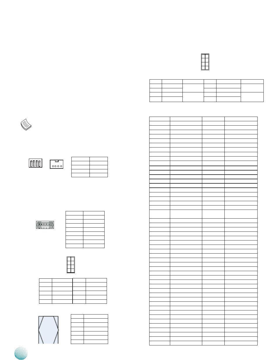
Mini PCI Express Connector (MIO1) on the mainboard:
COM and Audio Expansion Card Connector
PIN
Pin Name
PIN
Pin Name
1
GNd
51
HdA_BCLK
2
sATATXN2
52
HdA_sYNC
3
sATATXP2
53
HdA_RsT
4
GNd
54
HdA_sdIN0
5
sATARXN2
55
HdA_sdO
6
sATARXP2
56
sPK
7
GNd
57
VCC3_sB
8
VCC3P3_Ps
58
VCC3_sB
9
VCC3P3_Ps
59
VCC3_sB
10
VCC3P3_Ps
60
VCC3_sB
11
GNd
61
VCC3_sB
12
PCIE_RXN5
62
PCIE_RXN6
13
PCIE_RXP5
63
PCIE_RXP6
14
PCIE_TXN5
64
PCIE_TXN6
15
PCIE_TXP5
65
PCIE_TXP6
16
PCIE_CKN5
66
PCIE_CKN6
17
PCIE_CKP5
67
PCIE_CKP6
18
IGN_dI2
68
IGN_dI1
19
PLTRsT
69
sMBCLK_
20
WAKE_N
70
sMBdATA
21
dCIN_VCC
71
REMOTE_POWER_
ON
22
VCC12_Ps
72
3G_POWER_ON
23
VCC5_sB
73
UsB_N12
24
VCC5_sB
74
UsB_P12
25
VCC5
75
GNd
26
VCC5
76
UsB_N13
27
VCC5
77
UsB_P13
28
GNd
78
GNd
29
dGOUT_0
79
dGIN_0
30
dGOUT_1
80
dGIN_1
31
dGOUT_2
81
dGIN_2
32
dGOUT_3
82
dGIN_3
33
GNd
83
GNd
34
COM3_dCd#
84
COM1_dCd#
35
COM3_RI#
85
COM1_RI#
36
COM3_CTs#
86
COM1_CTs#
37
COM3_dTR#
87
COM1_dTR#
38
COM3_RTs#
88
COM1_RTs#
39
COM3_dsR#
89
COM1_dsR#
40
COM3_sOUT
90
COM1_sOUT
41
COM3_sIN
91
COM1_sIN
42
GNd
92
GNd
43
COM4_dCd#
93
COM2_dCd#
44
COM4_RI#
94
COM2_RI#
45
COM4_CTs#
95
COM2_CTs#
46
COM4_dTR#
96
COM2_dTR#
47
COM4_RTs#
97
COM2_RTs#
48
COM4_dsR#
98
COM2_dsR#
49
COM4_sOUT
99
COM2_sOUT
50
COM4_sIN
100
COM2_sIN
10
8
6
4
2
9
7
5
3
1
Pin No.
description
C1
UIM_PWR
C2
UIM_RsT
C3
UIM_CLK
C5
GNd
C6
UIM_VPP
C7
UIM_dAT
C5 C7
C1 C3
1 2 3 4
5 6 7 8
Pin No.
Pin Name
1
VCCUsB
2
UsB0N
3
UsB0P
4
GNd
5
VCCUsB1
6
UsB1N
7
UsB1P
8
GNd
Pin No. Pin Name
1
VCCUsB10
3
N/A
5
UsB10N
7
UsB10P
9
GNd
Pin No. Pin Name
2
GNd
4
UsB11P
6
UsB11N
8
N/A
10
VCCUsB11
1
3
5
7
9
2
4
6
8
10
Pin No.
Function
1
+12V
2
GNd
3
GNd
4
+5V
Pin No. Pin Name
Function
Pin No.
Pin Name
Function
1
Hd_LEd+
Hdd LEd
2
PWR_LEd+
Power LEd
3
Hd_LEd-
4
PWR_LEd-
5
Reset
system Reset
Button
6
POWER_BTN Power On/Off
Push Button
7
GNd
8
GNd
4 3 2 1