Typical applications – Linx Technologies TRM-xxx-TT User Manual
Page 21
– –
– –
36
37
Typical Applications
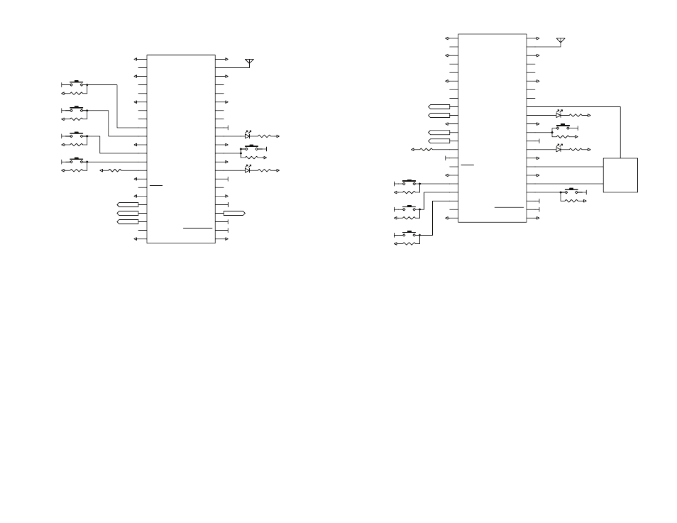
Figure 31 and Figure 32 show circuits using the TT Series transceiver.
In this example, C0 is high and C1 is low, so S0–S3 are inputs and S4–S7
are outputs. The inputs are connected to buttons that pull the lines high
and weak pull-down resistors to keep the lines from floating when the
buttons are not pressed. The outputs would be connected to external
application circuitry.
LATCH_EN is low, so the outputs are momentary.
The Command Data Interface is not used in this design, so CMD_DATA_IN
is tied high and CMD_DATA_OUT is not connected.
ACK_OUT and MODE_IND are connected to LEDs to provide visual
indication to the user.
PAIR is connected to a button and pull-down resistor to initiate the Pair
Process when the button is pressed.
ACK_EN is tied high so the module sends acknowledgements as soon as it
receives a control message.
1
TRM-XXX-TT
NC
2
GND
3
NC
4
NC
5
GND
6
NC
7
S0
9
S1
10
GND
11
S7
18
S6
19
RSSI
21
GND
22
GND
23
POWER_DOWN
24
VCC
25
S5
26
CMD_DATA_IN
27
S2
12
GND
17
S3
13
LVL_ADJ
14
LATCH_EN
15
RESET
16
NC
8
S4
20
GND
GND
28
CMD_DATA_OUT
29
C0
30
ACK_OUT
31
C1
32
PAIR
33
GND
34
MODE_IND
35
ACK_EN
36
NC
37
NC
38
GND
39
NC
40
NC
41
GND
42
ANTENNA
43
GND
44
GND
GND
GND
GND
GND
GND
GND
GND
GND
GND
GND
GND
VCC
VCC
GND
100k
100k
100k
100k
GND
91k 1%
GND
GND
GND
GND
VCC
VCC
VCC
VCC
GND
S7
S6
S4
S5
VCC
GND
GND
GND
VCC
VCC
NC
2
GND
3
NC
4
NC
5
GND
6
NC
7
S0
9
S1
10
GND
11
S7
18
S6
19
RSSI
21
GND
22
GND
23
POWER_DOWN
24
VCC
25
S5
26
CMD_DATA_IN
27
S2
12
GND
17
S3
13
LVL_ADJ
14
LATCH_EN
15
RESET
16
NC
8
S4
20
GND
1
GND
28
CMD_DATA_OUT
29
C0
30
ACK_OUT
31
C1
32
PAIR
33
GND
34
MODE_IND
35
ACK_EN
36
NC
37
NC
38
GND
39
NC
40
NC
41
GND
42
ANTENNA
43
GND
44
TRM-XXX-TT
GND
GND
GND
GND
GND
GND
GND
GND
GND
GND
GND
GND
VCC
VCC
GND
91k 1%
GND
S0
S1
S2
S3
VCC
GND
GND
100k
GND
VCC
100k
100k
100k
GND
GND
GND
GND
VCC
VCC
VCC
VCC
VCC
100k
µ
VCC
RX
TX
GPIO
100k
Figure 31: TT Series Transceiver Basic Application Circuit
In this example, C0 is low and C1 is high, so S0–S3 are outputs and
S4–S7 are inputs. This is inverted from the circuit in Figure 31 making it the
matching device.
In this circuit, the Command Data Interface is connected to a
microcontroller for using some of the advanced features.
The microcontroller controls the state of the ACK_EN line. it can receive
a command, perform an action and then take the line high to send
Acknowledgement packets. This lets the user on the other end know that
the action took place and not just that the command was received.
1
TRM-XXX-TT
NC
2
GND
3
NC
4
NC
5
GND
6
NC
7
S0
9
S1
10
GND
11
S7
18
S6
19
RSSI
21
GND
22
GND
23
POWER_DOWN
24
VCC
25
S5
26
CMD_DATA_IN
27
S2
12
GND
17
S3
13
LVL_ADJ
14
LATCH_EN
15
RESET
16
NC
8
S4
20
GND
GND
28
CMD_DATA_OUT
29
C0
30
ACK_OUT
31
C1
32
PAIR
33
GND
34
MODE_IND
35
ACK_EN
36
NC
37
NC
38
GND
39
NC
40
NC
41
GND
42
ANTENNA
43
GND
44
GND
GND
GND
GND
GND
GND
GND
GND
GND
GND
GND
GND
VCC
VCC
GND
100k
100k
100k
100k
GND
91k 1%
GND
GND
GND
GND
VCC
VCC
VCC
VCC
GND
S7
S6
S4
S5
VCC
GND
GND
GND
VCC
VCC
NC
2
GND
3
NC
4
NC
5
GND
6
NC
7
S0
9
S1
10
GND
11
S7
18
S6
19
RSSI
21
GND
22
GND
23
POWER_DOWN
24
VCC
25
S5
26
CMD_DATA_IN
27
S2
12
GND
17
S3
13
LVL_ADJ
14
LATCH_EN
15
RESET
16
NC
8
S4
20
GND
1
GND
28
CMD_DATA_OUT
29
C0
30
ACK_OUT
31
C1
32
PAIR
33
GND
34
MODE_IND
35
ACK_EN
36
NC
37
NC
38
GND
39
NC
40
NC
41
GND
42
ANTENNA
43
GND
44
TRM-XXX-TT
GND
GND
GND
GND
GND
GND
GND
GND
GND
GND
GND
GND
VCC
VCC
GND
91k 1%
GND
S0
S1
S2
S3
VCC
GND
GND
100k
GND
VCC
100k
100k
100k
GND
GND
GND
GND
VCC
VCC
VCC
VCC
VCC
100k
µ
VCC
RX
TX
GPIO
100k
Figure 32: TT Series Transceiver Typical Application Circuit with External Microprocessor