Altera Phase-Locked Loop User Manual
Page 5
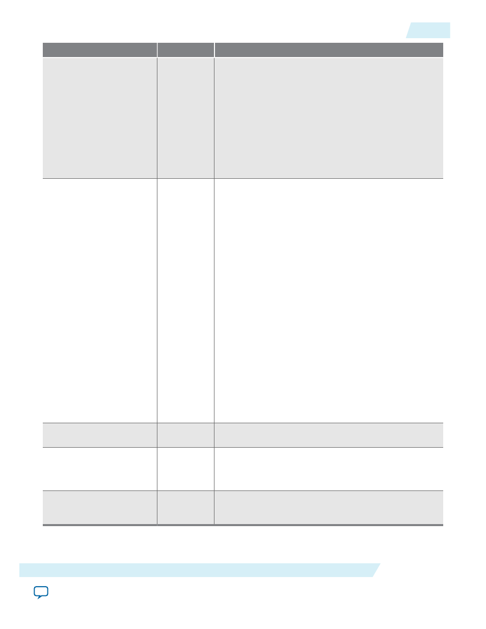
Parameter
Legal Value
Description
Second Reference Clock
Frequency
—
Selects the frequency of the second input clock signal. The
default value is 100.0 MHz. The minimum and maximum
value is dependent on the device used. The PLL reads only
the numerals in the first six decimal places.
The PLL is automatically configured to satisfy its legality
requirements for the primary reference clock only. If the
second reference clock frequency is different, this may cause
an illegal VCO or PFD frequency error. To avoid this error,
you can turn on Enable physical output clock parameters
and manually configure the PLL such that the frequency is
legal for both
refclk
inputs.
Switchover Mode
Automatic
Switchover,
Manual
Switchover, or
Automatic
Switchover
with Manual
Override
Specifies the switchover mode for design application. The IP
supports three switchover modes:
• If you select the Automatic Switchover mode, the PLL
circuitry monitors the selected reference clock. If one
clock stops, the circuit automatically switches to the
backup clock in a few clock cycles and updates the status
signals,
clkbad
and
activeclk
.
• If you select the Manual Switchover mode, when the
control signal,
extswitch
, changes from logic low to
logic high, and stays high for at least three clock cycles,
the input clock switches to the other clock. The
extswitch
can be generated from FPGA core logic or
input pin.
• If you select Automatic Switchover with Manual
Override mode, when the
extswitch
signal is high, it
overrides the automatic switch function. As long as
extswitch
remains high, further switchover action is
blocked. To select this mode, your two clock sources
must be running and the frequency of the two clocks
cannot differ by more than 20%. If both clocks are not on
the same frequency, but their period difference is within
20%, the clock loss detection block will detect the lost
clock. The PLL most likely drops out of lock after the
PLL clock input switchover and needs time to lock again.
Switchover Delay
0–7
Adds a specific amount of cycle delay to the switchover
process. The default value is 0.
Create an ‘active_clk’ signal
to indicate the input clock
in use
Turn on or
Turn off
Turn on to create the
activeclk
output. The
activeclk
output indicates the input clock which is in use by the PLL.
Output signal low indicates
refclk
and output signal high
indicates
refclk1
.
Create a ‘clkbad’ signal for
each of the input clocks
Turn on or
Turn off
Turn on to creates two
clkbad
outputs, one for each input
clock. Output signal low indicates the clock is working and
output signal high indicates the clock is not working.
UG-01087
2015.05.04
Altera PLL IP Core Parameters - Clock Switchover Tab
5
Altera Phase-Locked Loop (Altera PLL) IP Core User Guide
Altera Corporation