Figure 4–2 – Altera DSP Development Kit, Stratix V Edition User Manual
Page 19
Chapter 4: Development Board Setup
4–3
Factory Default Switch Settings
July 2013
Altera Corporation
DSP Development Kit, Stratix V Edition
User Guide
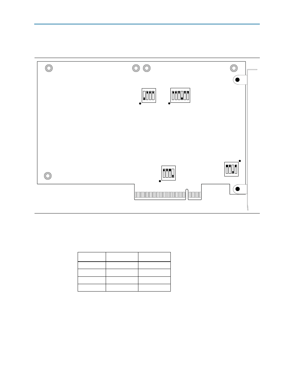
shows the switch locations and the default position of each switch on the
bottom side of the board.
To restore the switches to their factory default settings, perform the following steps:
1. Set jumper block (J8) to match
and
.
Figure 4–2. Switch Locations and Default Settings on the Board Bottom
4
3
2
1
ON
MSEL
6
5
4
3
2
1
ON
JTAG
4 3 2 1
SW5
ON
4
3
2
1
SW6
ON
x1 x4 x8
SECURITY FA
C
TO
R
Y
CLK_EN CLK_SEL
MAXV HSMA HSMB PCIE
ON = 0
OFF = 1
ON = 0
OFF = 1
SW3
SW4
Table 4–1. J8 Jumper Block
Jumper
HSMB VCCIO
Position
Pins 1-2
1.8 V
Not installed
Pins 3-4
1.5 V
Not installed
Pins 5-6
1.2 V
Not installed
No pins
2.5 V
Default
Note to
:
(1) Adding a single jumper between the pins sets the
voltage as described in the table. Install only one
jumper location at a time.