Max v registers, Max v registers –4, D. refer to – Altera DSP Development Kit, Stratix V Edition User Manual
Page 28: For an alter
6–4
Chapter 6: Board Test System
Using the Board Test System
DSP Development Kit, Stratix V Edition
July 2013
Altera Corporation
User Guide
■
Board Name
—Indicates the official name of the board.
■
Board P/N
—Indicates the part number of the board.
■
Serial number
—Indicates the serial number of the board.
■
Factory test version
—Indicates the version of the Board Test System currently
running on the board.
■
MAX V ver
—Indicates the version of MAX V code currently running on the
board. The MAX V code resides in the <install
dir>\kits\stratixVGS_5sgsmd5kf40_dsp\examples directory. Newer revisions of
this code might be available on
page
of the Altera website.
■
MAC
—Indicates the MAC address of the board.
MAX V Registers
The MAX V registers control allows you to view and change the current MAX V
register values as described in
. Changes to the register values with the GUI
take effect immediately.
■
SRST
—Resets the system and reloads the FPGA with a design from flash memory
based on the other MAX V register values. Refer to
for more information.
■
PSO
—Sets the MAX V PSO register. The following options are available:
■
Use PSR
—Allows the PSR to determine the page of flash memory to use for
FPGA reconfiguration.
■
Use PSS
—Allows the PSS to determine the page of flash memory to use for
FPGA reconfiguration.
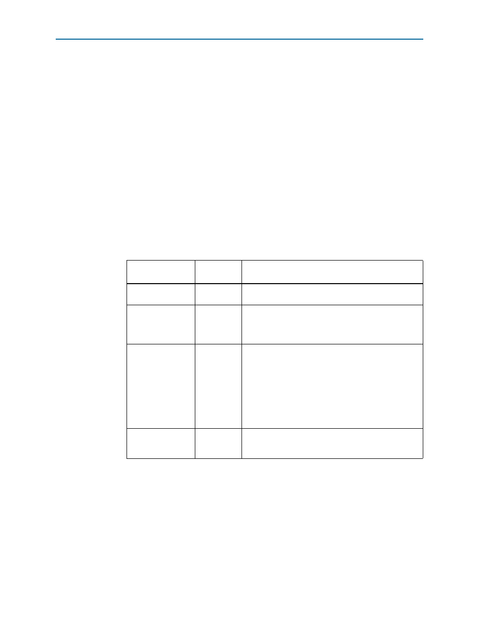
Table 6–1. MAX V Registers
Register Name
Read/Write
Capability
Description
System Reset
(SRST)
Write only
Set to 0 to initiate an FPGA reconfiguration.
Page Select Override
(PSO)
Read / Write
When set to 0, the value in PSR determines the page of
flash memory to use for FPGA reconfiguration. When set to
1, the value in PSS determines the page of flash memory to
use for FPGA reconfiguration.
Page Select Switch
(PSS)
Read only
Holds the current value of the illuminated PGM LED (D4-D6)
based on the following encoding:
■
0 = PGM LED (D6) and corresponds to the flash memory
page for the factory hardware design
■
1 = PGM LED (D5) and corresponds to the flash memory
page for the user hardware 1 design
■
2 = PGM LED (D4) and corresponds to the flash memory
page for the user hardware 2 design
Page Select Register
(PSR)
Read / Write
Determines which of the up to eight (0-7) pages of flash
memory to use for FPGA reconfiguration. The flash memory
ships with pages 0 and 1 preconfigured.