Altera PowerPlay Early Power Estimator User Manual
Page 30
3–16
Altera
Corporation
PowerPlay Early Power Estimator For Arria GX FPGAs
May 2008
PowerPlay Early Power Estimator Inputs
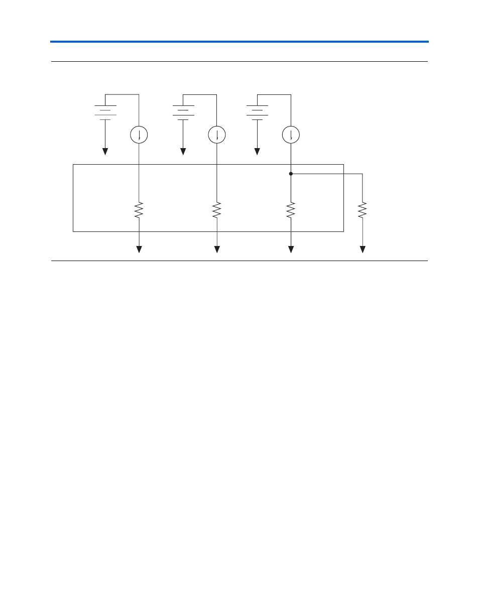
Figure 3–8. I/O Power Representation
The V
REF
pins consume minimal current (less than 10
μA) and is
negligible when compared to the power consumed by the general
purpose I/O pins. Therefore, the PowerPlay Early Power Estimator
spreadsheet does not include the current for V
REF
pins in the calculations.
Each row in the I/O section represents a design module where the I/O
pins have the same frequency, toggle percentage, average capacitive load,
I/O standard, drive strength, on-chip termination, data rate, and I/O
bank. You must enter the following parameters for each design module:
■
I/O standard
■
Drive strength/On-chip termination
■
Clock frequency (f
MAX
) in MHz
■
Number of output, input, and bidirectional pins
■
I/O bank
■
Pin toggle percentage
■
Output enable percentage
■
Average capacitance of the load
■
I/O data rate
V
CCINT
V
CCPD
V
CCIO
I
CCINT
I
CCPD
I
CCIO
Thermal P
INT
Thermal P
PD
Thermal P
IO
External P
IO
Arria GX Device