Max ii registers –6, Max ii registers – Altera Stratix IV GT 100G User Manual
Page 28
6–6
Chapter 6: Board Test System
Using the Board Test System
Stratix IV GT 100G Development Kit User Guide
October 2010
Altera Corporation
■
MAX II ver
—Indicates the version of MAX II code currently running on the board.
The MAX II code resides in the
<install dir>\kits\stratixIVGT_4sgt100g5_100g\examples directory. Newer
revisions of this code might be available on the
ge of the Altera website.
MAX II Registers
The MAX II registers control allow you to view and change the current MAX II
register values as described in
. Changes to the register values with the GUI
take effect immediately. For example, writing a 0 to SRST resets the board.
■
PSO
—Sets the MAX II PSO register. The following options are available:
■
Use PSR
—Allows the PSR to determine the page of flash memory to use for
FPGA reconfiguration.
■
Use PSS
—Allows the PSS to determine the page of flash memory to use for
FPGA reconfiguration.
■
PSR
—Sets the MAX II PSR register. The numerical values in the list corresponds to
the page of flash memory to load during FPGA reconfiguration. Refer to
for more information.
■
PSS
—Displays the MAX II PSS register value. Refer to
for the list of
available options.
■
SRST
—Resets the system and reloads the FPGA with a design from flash memory
based on the other MAX II register values. Refer to
for more information.
1
Because the Config tab requires that a specific design is running in the FPGA at a
specific clock speed, writing a 0 to SRST or changing the PSO value can cause the
Board Test System to stop running.
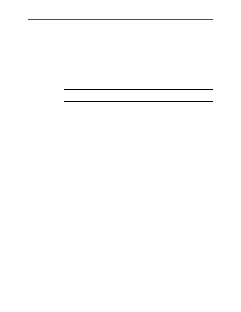
Table 6–1. MAX II Registers
Register Name
Read/Write
Capability
Description
System Reset
(SRST)
Write only
Set to 0 to initiate an FPGA reconfiguration.
Page Select Register
(PSR)
Read / Write
Determines which of the pages of flash memory to use for
FPGA reconfiguration. The flash memory ships with pages 0
and 1 preconfigured.
Page Select Override
(PSO)
Read / Write
When set to 0, the value in PSR determines the page of
flash memory to use for FPGA reconfiguration. When set to
1, the value in PSS determines the page of flash memory to
use for FPGA reconfiguration.
Page Select Switch
(PSS)
Read only
Holds the current value of the illuminated USER_POF LED
(D19, D20, D25) based on the following encoding:
■
0 = USER_POF1 LED (D19)
■
1 = USER_POF2 LED (D20)
■
2 = USER_POF3 LED (D25)