Jumper settings, Jumper settings 10, Chapter 3 – Lanner LEC-3010 User Manual
Page 12: Motherboard information
10
Motherboard Information
Chapter 3
Embedded and Industrial Computing
Jumper Settings
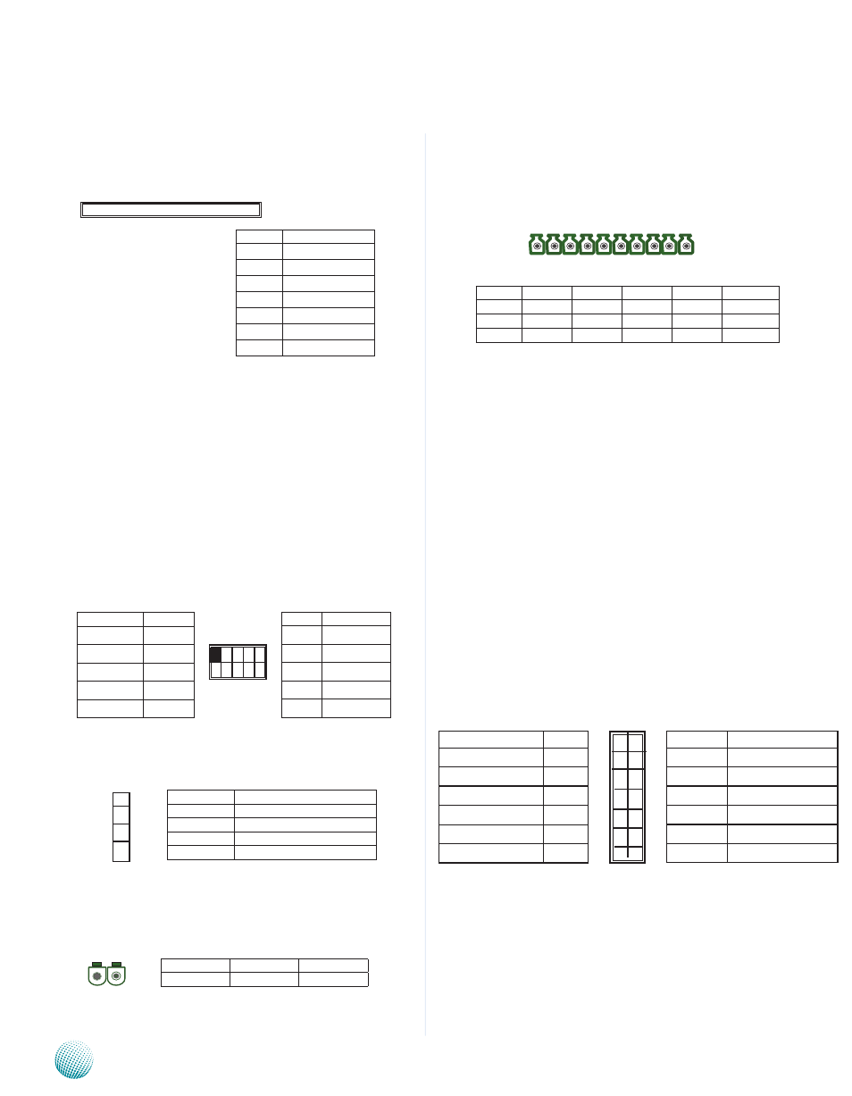
SATA (J1) : The system supports one SATA II drive
SODIMM1: The SO-DIMM socket is used to connect the
DDR2 667 (200 pin) memory The system can suport up to
2 GB in maximum
ATX12V1: The system is designed to operate with a single
DC input with voltage range from +12 to 36V And it is
supplied through the Phoenix Contact This connector is
provided for the main board to recevie power from the
input source
SATA Power (J5): 4 Pin SATA Power Connector
CN1(on DC/DC converter board): A power socket for a
power supply through Phoenix Contact
U46: This connector provides 4 digital inputs and 4 digital
outputs The connector type of LEC-3010 is plug-in screw
terminal block that enables you to connect to field I/O
devices directly
Digital Inputs Requirements
Digital Input/Output Requirements
Input /Output Voltage:
Logic 0: 0 ~ 2V DC
Logic 1: 2 ~ 5V DC
Current limit: Maximum 100mA for each pin
VGA Connector (J6): The system has an integrated
graphics processing unit (GPU) from Intel’s Graphics Media
Accelerator It has the following features:
A D-sub 15-pin connector to support a VGA CRT
•
monitor It supports resolution up to 1024 x 768
@60-Hz
Intel Dynamic Video Memory Technology 4 0
•
Intel Clear Video Technology consisted of MPEG2
•
Hardware Acceleration and ProcAmp
1 2 3 4 5 6 7
Pin No.
Function
1
GND
2
TX_P
3
TX_M
4
GND
5
RX_M
6
RX_P
7
GND
Function
Pin No.
NC
1
GND
3
GND
5
GND
7
GND
9
Pin No.
Function
2
12V
4
12V
6
12V
8
12V
10
12V
1 3 5 7 9
2 4 6 8 10
1 2 3 4 5 6 7 8 9 1 0
Pin No.
1
2
3
4
5
Function
GND
FP_DI_0
FP_DI_1
FP_DI_2
FP_DI_3
Pn No.
6
7
8
9
10
Function
GND
F_GPO0
F_GPO1
F_GPO2
F_GPO3
Pin No.
Function
1
5V
2
Ground
3
Ground
4
12V
4
3
2
1
Pin No.
1
2
Function
Ground
DC=In
12
Pin Name
Pin No.
R
1
G
3
B
5
H-SYNC
7
V-SYNC
9
Detect-display Data
11
Pin No.
Pin Name
2
GND
4
GND
6
GND
8
GND
10
GND
12
Detect-display Clock
1
3
5
7
9
11
2
4
6
8
10
12