Chapter 3, Motherboard information – Lanner LEC-3010 User Manual
Page 13
11
Motherboard Information
Chapter 3
Embedded and Industrial Computing
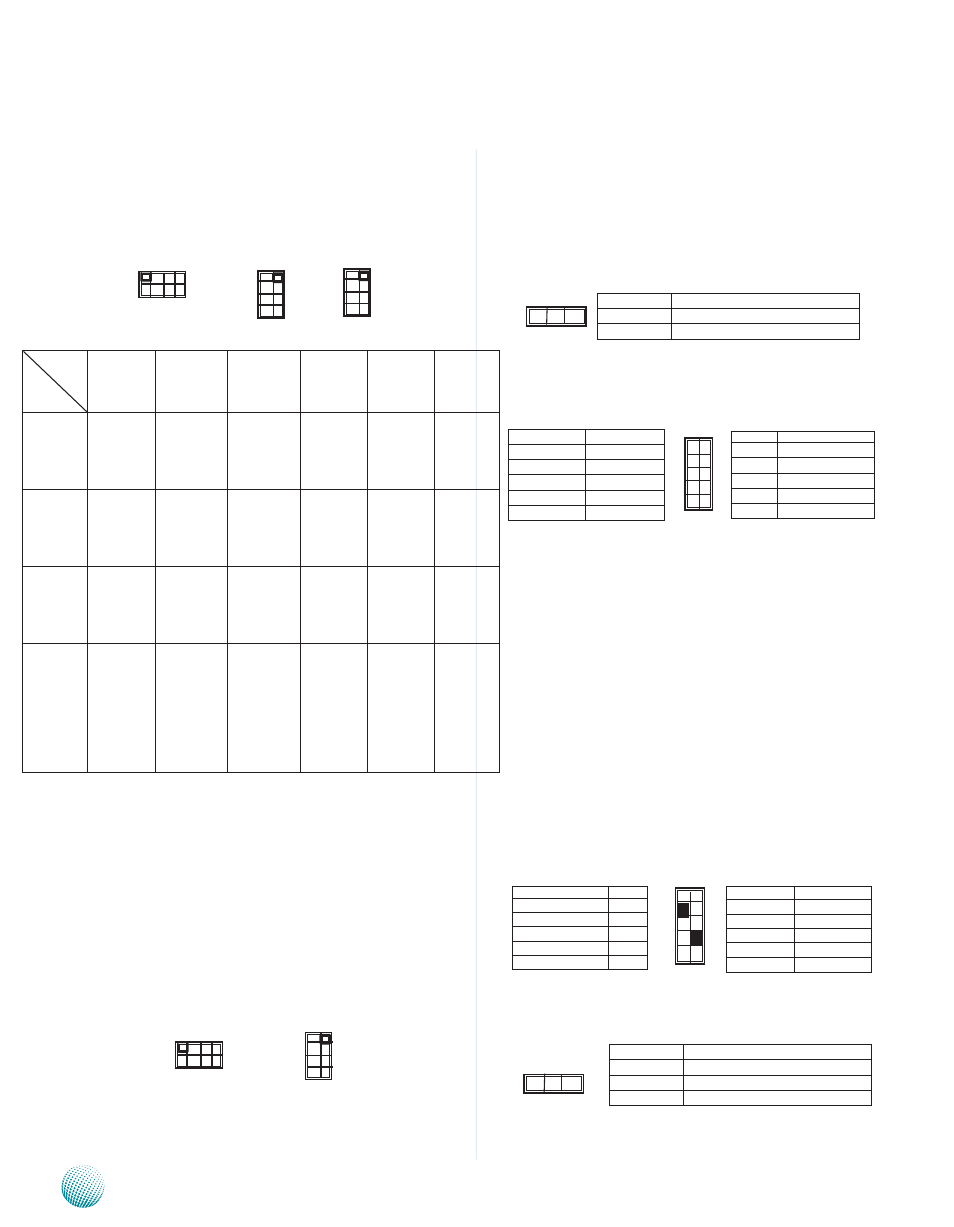
Clear CMOS (JP1): The motherboard contains a jumper
that can erase CMOS data and reset the systemBIOS
information Normally this jumper should be set with
pins 1-2 closed If you want to reset the CMOS data, set
this jumper to 2-3 closed for just a few seconds, and then
move the jumper back to 1-2 closed This procedure will
reset the CMOS to its default setting
SPI-ROM(J2): Using the appropriate cable to connect this
10-pin ISP in header connector, the user can update the
SPI Flash soldered on board
CN2: Connector CN2 together with U79 provide access to
the COM1 through COM6 serial port’s data transmission
when the port is configured for either RS-422/RS-485
or RS-232 serial protocol The signals present on each
of the connector’s pins for these three modes can be
referenced in Front Panel Features, Chapter 1 Introduction
The COM ports' serial protocol mode is configured using
the following dip switches: SW3, SW4, SW7, SW8, SW16,
and SW17 In addition, when used as in RS-485 mode, the
system can automatically detect the direction of incoming
data and switches its transmission direction accordingly –
the automatic data flow control in RS-485
USBF1: Dual USB Interface Connector It is used for
connecting the USB module cable It complies with USB2 0
and support up to 480 Mbps connection speed
System Management Bus (J3)
SW3/SW4/SW7/SW8/SW16/SW17: These switches —
SW3, SW4, SW7, SW8, SW16 and SW17 — are used to
adjust the serial port type for COM1, COM2, COM3, COM4,
COM5, and COM6 respectively Use the table below as the
switch adjustment information for COM1 through COM4
SW2/SW5/SW6/SW9/SW11/SW14: Switches — SW2,
SW5, SW6, SW9, SW11, and SW14 — are used to enable
or disable the signal termination for COM1, COM2, COM3,
COM4, COM5, and COM6 respectively Look up at the last
row of the above table for the dip switch adjustment for
COM1 through COM6 We strongly recommded that you
disable termination when the port is configured as RS-232
and enable it when the port is configured as RS-485/RS-
422
3 2 1
Pin No.
Function
Short 1-2
Normal (Default)
2-3
Clear CMOS
ON
1 2 3 4
OFF
C O M
P o r t
No.
Port Type
COM 1
COM 2
COM 3
COM 4
COM 5
COM 6
RS-232
Switch 3:
1 ON
2 OFF
3 OFF
4 OFF
Switch 8:
1 ON
2 OFF
3 OFF
4 OFF
Switch 4:
1 ON
2 OFF
3 OFF
4 OFF
Switch 7:
1 ON
2 OFF
3 OFF
4 OFF
Switch 16
1 ON
2 OFF
3 OFF
4 OFF
Switch 17
1 ON
2 OFF
3 OFF
4 OFF
RS-422
Switch 3:
1 OFF
2 ON
3 ON
4 OFF
Switch 8:
1 OFF
2 ON
3 ON
4 OFF
Switch 4:
1 OFF
2 ON
3 ON
4 OFF
Switch 7:
1 OFF
2 ON
3 ON
4 OFF
Switch 16
1 OFF
2 ON
3 ON
4 OFF
Switch 17
1 OFF
2 ON
3 ON
4 OFF
RS-485
Switch 3:
1 OFF
2 ON
3 OFF
4 ON
Switch 8:
1 OFF
2 ON
3 OFF
4 ON
Switch 4:
1 OFF
2 ON
3 OFF
4 ON
Switch 7:
1 OFF
2 ON
3 OFF
4 ON
Switch 16:
1 OFF
2 ON
3 OFF
4 ON
Switch 17:
1 OFF
2 ON
3 OFF
4 ON
Termina-
tion
(Enable/dis-
able)
Switch 2:
Enable ON
1 ON
2 ON
3 ON
4 ON
Disable: OFF
Switch 9
Enable ON
1 ON
2 ON
3 ON
4 ON
Disable: OFF
Switch 5:
Enable ON
1 ON
2 ON
3 ON
4 ON
Disable: OFF
Switch 6:
Enable ON
1 ON
2 ON
3 ON
4 ON
Disable: OFF
Switch 11:
Enable ON
1 ON
2 ON
3 ON
4 ON
Disable: OFF
Switch 14:
Enable ON
1 ON
2 ON
3 ON
4 ON
D i s a b l e :
OFF
Pin No.
Function
2
RSVD
4
VCC3P3_SB_SPI
6
RSVD
8
SPI_CLK
10
SPI_MOSI
Function
Pin No.
SPI_HOLD_N
1
SPI_CS0_N
3
SPI_MISO
5
RSVD
7
GND
9
1
3
5
7
9
2
4
6
8
10
Pin Name
Pin No.
USB_VCC
1
Key
3
USBD0-
5
USBD0+
7
GND
9
Pin No.
Pin Name
2
GND
4
USBD1+
6
USBD1-
8
Key
10
USB_VCC
1
3
5
7
9
2
4
6
8
10
1 2 3
Pin No.
Function
1
ICH_SMBDAT
2
Ground
3
ICH_SMBCLK
ON
OFF
1
2
3
4
4
3
2
1
ON OFF
SW16
SW17
ON
OFF
1
2
3
4
SW11/SW14
ON
1 2 3 4
OFF