Table 6.31 external memory read, External memory read – Avago Technologies LSI53C896 User Manual
Page 307
Advertising
PCI and External Memory Interface Timing Diagrams
6-39
Version 3.3
Copyright © 1998–2003 by LSI Logic Corporation. All rights reserved.
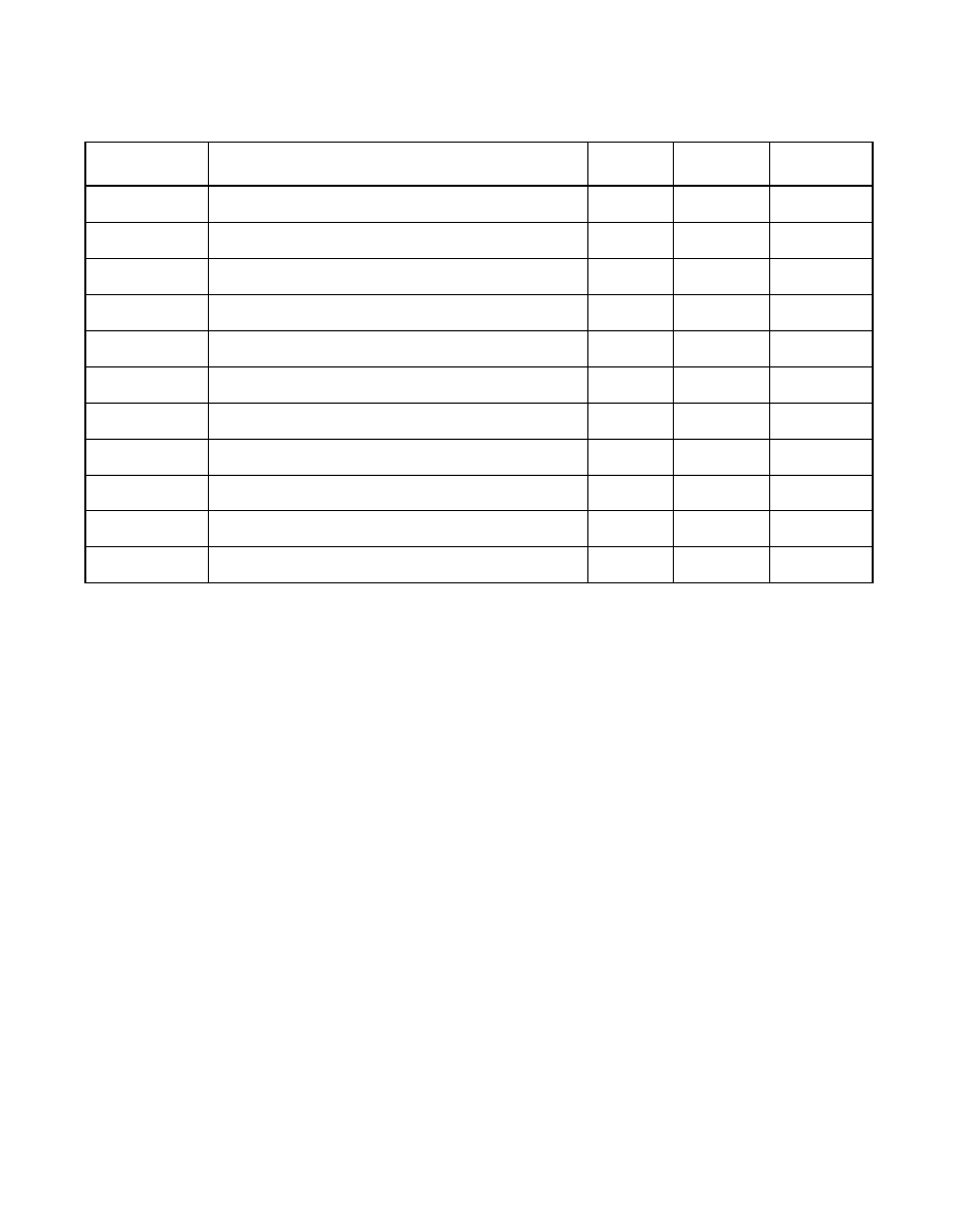
Table 6.31
External Memory Read
Symbol
Parameter
Min
Max
Unit
t
1
Shared signal input setup time
7
–
ns
t
2
Shared signal input hold time
0
–
ns
t
3
CLK to shared signal output valid
–
11
ns
t
11
Address setup to MAS/ HIGH
25
–
ns
t
12
Address hold from MAS/ HIGH
15
–
ns
t
13
MAS/ pulse width
25
–
ns
t
14
MCE/ LOW to data clocked in
160
–
ns
t
15
Address valid to data clocked in
205
–
ns
t
16
MOE/ LOW to data clocked in
100
–
ns
t
17
Data hold from address, MOE/, MCE/ change
0
–
ns
t
19
Data setup to CLK HIGH
5
–
ns
Advertising