Cyclone iii ls fpga clock outputs, Cyclone iii ls fpga clock outputs –22 – Altera Cyclone III LS FPGA Development Board User Manual
Page 30
2–22
Chapter 2: Board Components
Clock Circuitry
Cyclone III LS FPGA Development Board Reference Manual
© October 2009 Altera
Corporation
Cyclone III LS FPGA Clock Outputs
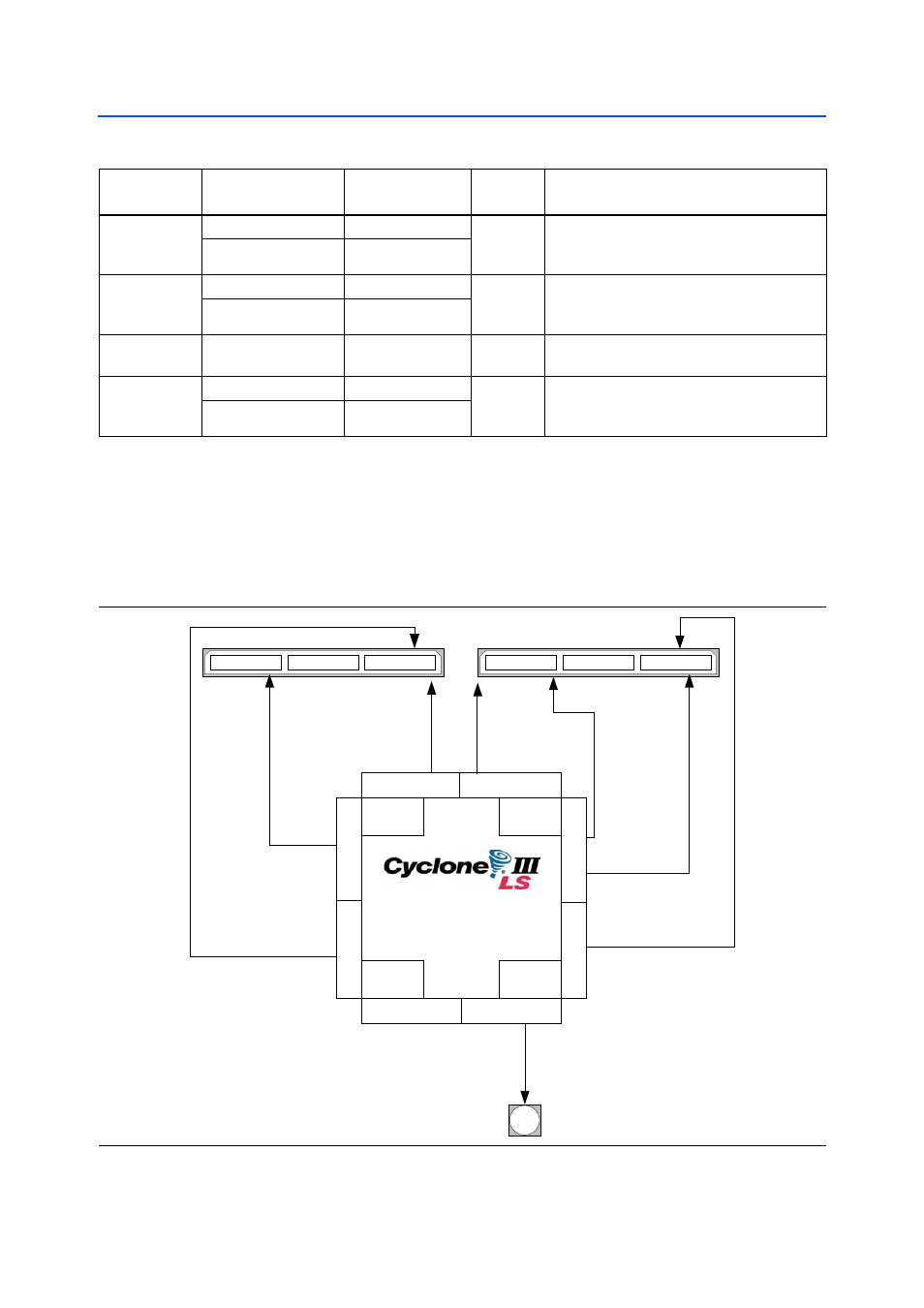
shows the Cyclone III LS FPGA development board clock outputs.
Samtec HSMC
HSMA_CLKIN_P1
AG16
LVTTL
LVTTL inputs from the installed HSMC port A
cable or board. Can also support LVDS inputs
when the termination resistor is installed.
HSMA_CLKIN_N1
AH16
Samtec HSMC
HSMA_CLKIN_P2
T27
LVTTL
LVTTL input from the installed HSMC port A
cable or board. Can also support LVDS inputs.
when the termination resistor is installed
HSMA_CLKIN_N2
T28
Samtec HSMC
HSMB_CLKIN0
B13
LVTTL
Single-ended input from the installed HSMC
port B cable or board.
Samtec HSMC
HSMB_CLKIN_P2
T2
LVTTL
LVTTL input from the installed HSMC port B
cable or board. Can also support LVDS inputs
when the termination resistor is installed.
HSMB_CLKIN_N2
T1
Note to
:
(1) CDCM61001 has a default frequency of 125 MHz, but can also be set to frequencies of 100 MHz, 150 MHz, and 156.25 MHz by the MAX II CPLD
EPM2210 System Controller..
Table 2–20. Cyclone III LS FPGA Development Board Clock Inputs (Part 2 of 2)
Source
Schematic Signal
Name
Cyclone III LS
Device Pin Number
I/O
Standard
Description
Figure 2–7. Cyclone III LS FPGA Development Board Clock Outputs
7 6 5 4 3 2 1 0
7 6 5 4 3 2 1 0
HSMA_CLKOUT_P[2]/N[2]
CLKOUT_SMA
SMA
DDR2_B7_CLK_P/N
(1.8V
SS
TL)
(2.5 V)
PLL 1
PLL 3
PLL 2
PLL 4
EP3CLS200F780
Bank 8
Bank 7
Bank 3
Bank 4
Bank 1
Bank 2
Bank 6
Bank 5
EP3CLS70F780
Migratable to
(LVDS)
HSMA_CLKOUT_P[1]/N[1]
(LVDS)
H
S
MA_CLKOUT0
(2.5 V)
DDR2_B8_CLK_P/N
(1.8V
SS
TL)
HSMB_CLKOUT_P[2]/N[2]
(LVDS)
HSMB
HSMB
H
S
MB_CLKOUT0
(2.5 V)