Altera Cyclone III LS FPGA Development Board User Manual
Page 50
2–42
Chapter 2: Board Components
Memory
Cyclone III LS FPGA Development Board Reference Manual
© October 2009 Altera
Corporation
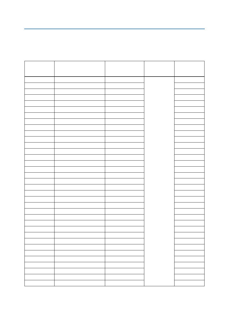
lists the flash pin assignments, signal names, and functions. The signal
names and types are relative to the Cyclone III LS device in terms of I/O setting and
direction.
Table 2–42. Flash Pin Assignments, Schematic Signal Names, and Functions (Part 1 of 2)
Board Reference
Description
Schematic Signal Name
I/O Standard
Cyclone III LS
Device
Pin Number
U9.F6
Address valid
FLASH_ADVn
2.5-V
AF18
U9.B4
Chip enable
FLASH_CEn
AH22
U9.E6
Clock
FLASH_CLK
AH6
U9.F8
Output enable
FLASH_OEn
AD7
U9.F7
Ready
FLASH_RDYBSYn
V4
U9.D4
Reset
FLASH_RESETn
AH5
U9.G8
Write enable
FLASH_WEn
AH17
U9.C6
Address valid
FLASH_WPn
—
U9.A1
Address bus
FSM_A1
AD14
U9.B1
Address bus
FSM_A2
AA17
U9.C1
Address bus
FSM_A3
AE12
U9.D1
Address bus
FSM_A4
AF21
U9.D2
Address bus
FSM_A5
AH2
U9.A2
Address bus
FSM_A6
AB12
U9.C2
Address bus
FSM_A7
AG24
U9.A3
Address bus
FSM_A8
AE25
U9.B3
Address bus
FSM_A9
AH21
U9.C3
Address bus
FSM_A10
AD25
U9.D3
Address bus
FSM_A11
AC9
U9.C4
Address bus
FSM_A12
AF4
U9.A5
Address bus
FSM_A13
AE10
U9.B5
Address bus
FSM_A14
AH26
U9.C5
Address bus
FSM_A15
AG22
U9.D7
Address bus
FSM_A16
AF12
U9.D8
Address bus
FSM_A17
AE19
U9.A7
Address bus
FSM_A18
AA9
U9.B7
Address bus
FSM_A19
AE6
U9.C7
Address bus
FSM_A20
AG18
U9.C8
Address bus
FSM_A21
AE11
U9.A8
Address bus
FSM_A22
AB16
U9.G1
Address bus
FSM_A23
AE13
U9.H8
Address bus
FSM_A24
AG11
U9.B6
Address bus (die select)
FSM_A25
AE9
U9.F2
Data bus
FSM_D0
AH9
U9.E2
Data bus
FSM_D1
AH24