Table 2–29 – Altera Cyclone III LS FPGA Development Board User Manual
Page 34
2–26
Chapter 2: Board Components
General User Input/Output
Cyclone III LS FPGA Development Board Reference Manual
© October 2009 Altera
Corporation
shows the LCD pin definitions, and is an excerpt from the Lumex data
sheet.
f
For more information such as timing, character maps, interface guidelines, and other
related documentation, visi
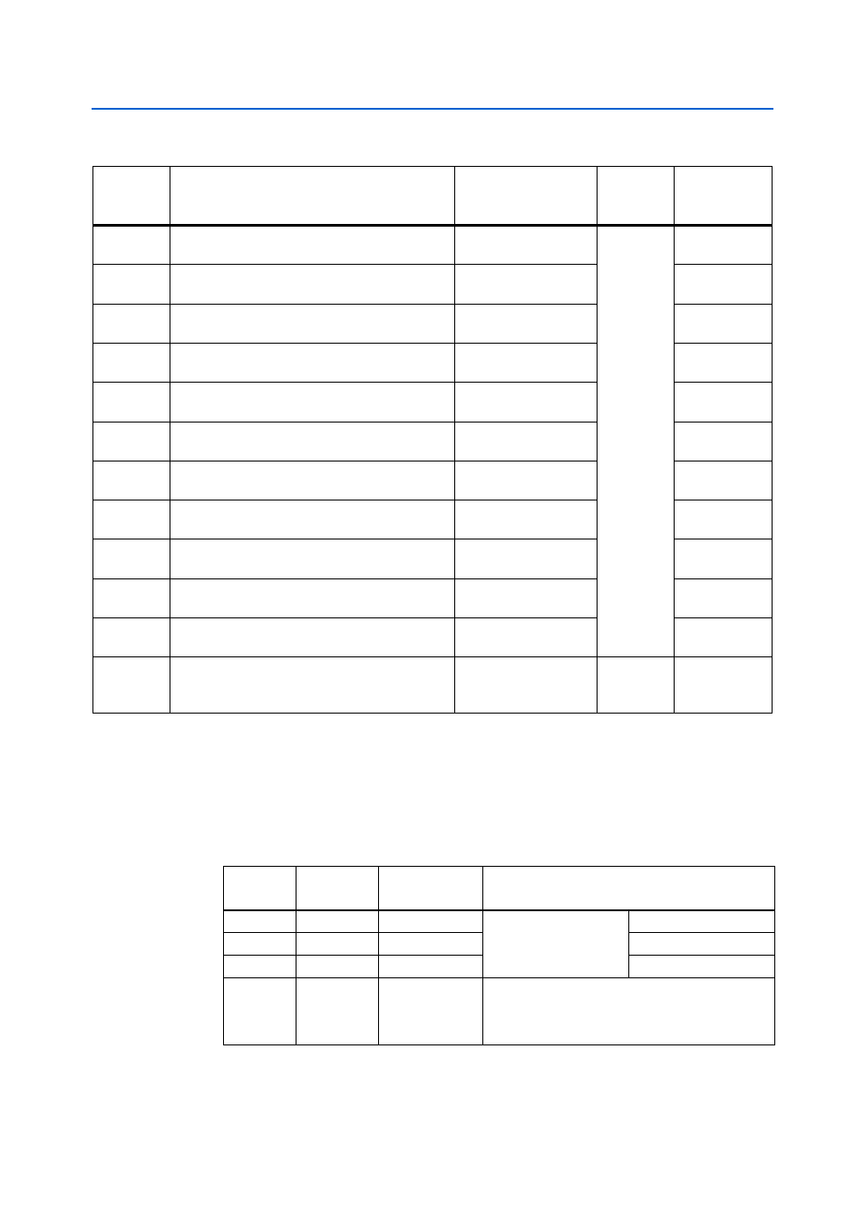
Table 2–29. LCD Pin Assignments, Schematic Signal Names, and Functions
Board
Reference
Description
Schematic Signal
Name
I/O
Standard
Cyclone III LS
Device
Pin Number
J19.4
LCD chip select (LCD_CSn) when
LCD_HSMB_SEL
is set to a logic 0.
LCD_HSMB_D[65]
2.5-V
P1
J19.11
LCD data bus bit 4 (LCD_DATA4) when
LCD_HSMB_SEL
is set to a logic 0.
LCD_HSMB_D[66]
AE4
J19.5
LCD write enable (LCD_WEn) when
LCD_HSMB_SEL
is set to a logic 0.
LCD_HSMB_D[67]
J4
J19.14
LCD data bus bit 7 (LCD_DATA7) when
LCD_HSMB_SEL
is set to a logic 0.
LCD_HSMB_D[68]
AE1
J19.12
LCD data bus bit 5 (LCD_DATA5) when
LCD_HSMB_SEL
is set to a logic 0.
LCD_HSMB_D[69]
AF1
J19.13
LCD data bus bit 6 (LCD_DATA6) when
LCD_HSMB_SEL
is set to a logic 0.
LCD_HSMB_D[70]
AD2
J19.4
LCD data or command select (LCD_D_Cn) when
LCD_HSMB_SEL
is set to a logic 0.
LCD_HSMB_D[71]
L1
J19.7
LCD data bus bit 0 (LCD_DATA0) when
LCD_HSMB_SEL
is set to a logic 0.
LCD_HSMB_D[72]
V5
J19.8
LCD data bus bit 1 (LCD_DATA1) when
LCD_HSMB_SEL
is set to a logic 0.
LCD_HSMB_D[73]
W4
J19.10
LCD data bus bit 3 (LCD_DATA3) when
LCD_HSMB_SEL
is set to a logic 0.
LCD_HSMB_D[74]
W6
J19.9
LCD data bus bit 2 (LCD_DATA2) when
LCD_HSMB_SEL
is set to a logic 0.
LCD_HSMB_D[75]
W7
J18
To control the LCD via the FPGA, a shunt should
be placed on this jumper, or the FPGA must drive
a logic 0.
LCD_HSMB_SEL
1.8-V
D20
Table 2–30. LCD Pin Definitions and Functions (Part 1 of 2)
Pin
Number
Symbol
Level
Function
1
V
DD
—
Power supply
5 V
2
V
SS
—
GND (0 V)
3
V
0
—
For LCD drive
4
RS
H/L
Register select signal
H: Data input
L: Instruction input