Eeprom, Eeprom –43 – Altera Cyclone III LS FPGA Development Board User Manual
Page 51
Chapter 2: Board Components
2–43
Memory
© October 2009 Altera Corporation
Cyclone III LS FPGA Development Board Reference Manual
lists the flash component reference and manufacturing information.
EEPROM
A 32-Kbit I
2
C serial EEPROM is accessible from the Cyclone III LS device. The
EEPROM speed is between 100 KHz and 400 KHz.
lists the EEPROM pin assignments, signal names, and functions. The signal
names and types are relative to the Cyclone III LS device in terms of I/O setting and
direction.
U9.G3
Data bus
FSM_D2
2.5-V
AF25
U9.E4
Data bus
FSM_D3
AE5
U9.E5
Data bus
FSM_D4
AB11
U9.G5
Data bus
FSM_D5
AD24
U9.G6
Data bus
FSM_D6
AF9
U9.H7
Data bus
FSM_D7
AE7
U9.E1
Data bus
FSM_D8
AE23
U9.E3
Data bus
FSM_D9
AF15
U9.F3
Data bus
FSM_D10
AD17
U9.F4
Data bus
FSM_D11
AF20
U9.F5
Data bus
FSM_D12
AH25
U9.H5
Data bus
FSM_D13
AE18
U9.G7
Data bus
FSM_D14
AD6
U9.E7
Data bus
FSM_D15
AG20
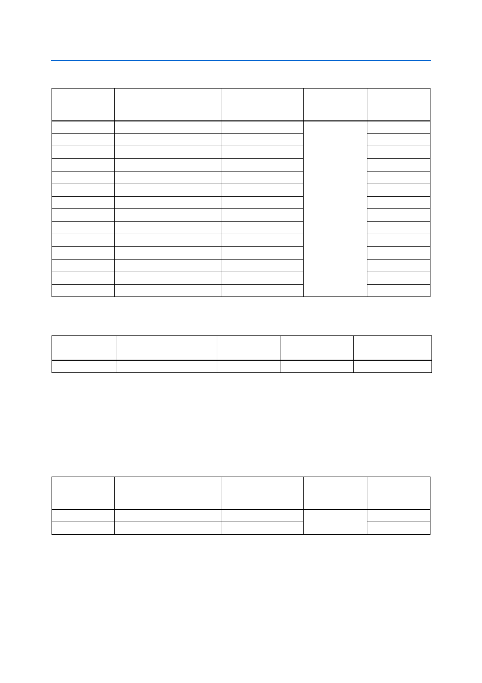
Table 2–42. Flash Pin Assignments, Schematic Signal Names, and Functions (Part 2 of 2)
Board Reference
Description
Schematic Signal Name
I/O Standard
Cyclone III LS
Device
Pin Number
Table 2–43. Flash Component Reference and Manufacturing Information
Board Reference
Description
Manufacturer
Manufacturing
Part Number
Manufacturer
Website
U9
512 Mbyte Synchronous Flash
Numonyx
PC48F4400P0VB00
Table 2–44. EEPROM Pin Assignments, Schematic Signal Names, and Functions
Board Reference
Description
Schematic Signal Name
I/O Standard
Cyclone III LS
Device
Pin Number
U21.6
EEPROM serial clock
EEPROM_SCL
2.5-V
AA3
U21.5
EEPROM serial data
EEPROM_SDA
AH3