Chapter 3: motherboard information, Block diagram, Chapter 3 – Lanner FW-8771 User Manual
Page 16: Motherboard information, Mb-8771a block diagram
11
Motherboard Information
Network Application Platforms
Chapter 3
Chapter 3:
Motherboard Information
Block Diagram
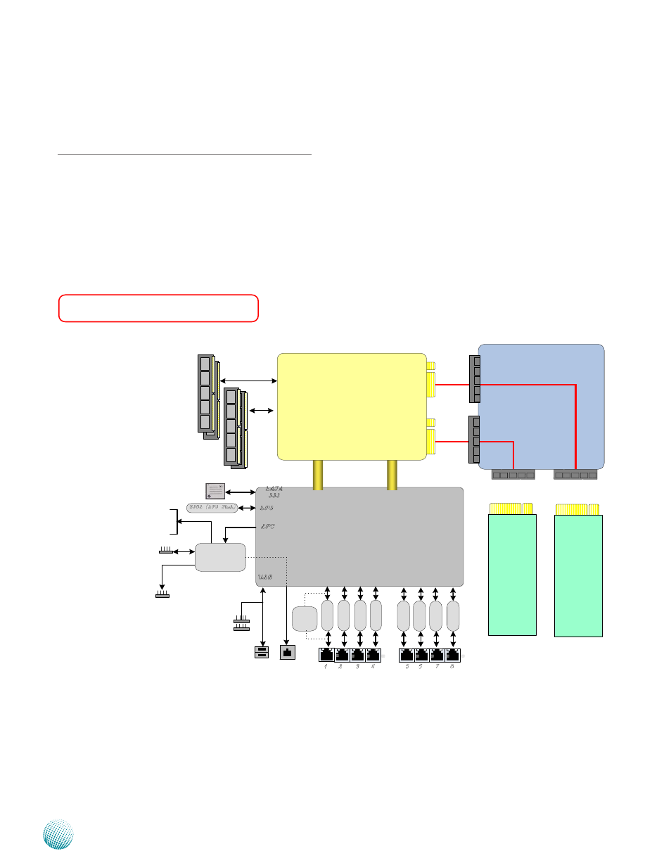
The block diagram depicts the relationships among the
interfaces or modules on the motherboard. Please refer
to the following figure for your motherboard’s layout
design.
RC-87111A
Intel C226
LynxPoint
(Compatible w/ H81)
FDI
(Direct Media Interface) X 4
DDR3 ECC/Non-ECC UDIMM memory for 1066/1333/1600MHz
Supports up to
32 GB
25.6 GB/sec (1600MHz)
25.6 GB/sec (1600MHz)
PCI-E x8 slot
For front
NIC module
NIC slot 2
PCI-E x8 slot
For front
NIC module
NIC slot 1
1 xGen3 PCI-E*8
Support Slim type NIC
MB-8771A Block Diagram
2xUSB 3.0
(front)
Console
8 x Gbe RJ45
3 Pairs bypass Gen.3 (from port 3~8)
PCI-E x8
OPMA
Parallel port for LCM module
GPIO
Fan Monitor
Thermal Monitor
NCT6776
cFast
IPMI / MGMT
For port 1
Intel Haswell
I7920
(LGA1150)
1 xGen3 PCI-E*8
2xUSB 3.0
(Internal)
Intel i210
(only support on FW-8771C)